FET as a Voltage Variable Resistor (VVR)
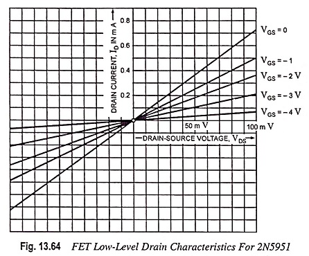
FET as a Voltage Variable Resistor (VVR): FET is a device that is usually operated in the constant-current portion of its output characteristics. But if it is operated in the region prior to pinch-off (i.e.,…
Comments Off on FET as a Voltage Variable Resistor (VVR)
November 15, 2022