Construction and Working of Zener Diode:
Zener diode, also sometimes called the breakdown diode, is a P-N junction diode specially designed for operation in the breakdown region in reverse bias condition. Construction and Working of Zener Diode is like an ordinary P-N junction diode except that it is properly doped so as to have a sharp breakdown voltage. The diode may use either zener breakdown mechanism or avalanche breakdown mechanism. Despite the fact that avalanche and zener constitute two types of breakdown diodes, the name zener is commonly applied to both types of diodes. The breakdown diode may be silicon or germanium one but silicon is preferred over germanium because of higher operating temperature and current capability. The knee point is also more sharp in case of a silicon diode. These diodes are analogous to gas discharge tubes in which large current appears on reaching the breakdown potential.
Zener diodes are connected into circuits with their cathodes as the positive terminal because they operate in the reverse-bias mode. Zener diodes are packaged in the same way as conventional semiconductor diodes. Small zener diodes are marked the same way as conventional diodes with a cathode band. The larger diodes are marked with the zener diode symbol shown in the illustration (Fig. 8.1). In addition to have a voltage rating (reverse breakdown), zener diodes have a power rating that must not be exceeded.
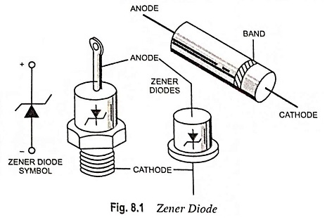
The symbol of a zener diode is given in Fig. 8.1. This is similar to that of a normal diode except that the line representing the cathode is bent at both ends i.e., the bar is turned into Z-shape; stands for zener.
Construction:
Construction of Zener Diode is like an ordinary P-N junction diode except that it is properly doped so as to have a sharp breakdown voltage. There are several methods used in the manufacture of zener diodes, such as diffused structure, diffused and passivated structure and alloy diffused structure.
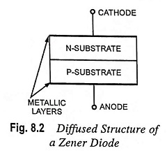
Diffused structure zener diode consists of two N and P substrates diffused together and has metallic layers deposited on both sides to connect anode and cathode terminals, as illustrated in Fig. 8.2. The drawback of such a construction is that the edges of the junction are exposed to contamination.
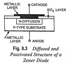
In passivated structure of a zener diode, the edges of the junction are covered by layer of SiO2, as illustrated in Fig. 8.3.
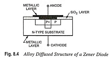
Similarly, all junctions are protected in alloy diffused structures, as shown in Fig. 8.4.
In general, the alloy diffused structure provides better zener characteristics at lower zener voltages. On the other hand, diffused and passivated zener diode is used at higher zener voltages.
Volt-Ampere Characteristics:
It has already been discussed that when the reverse bias on a crystal diode is gradually increased, a point is reached when the junction breaks down and a reverse current increases abruptly, as illustrated in Fig. 8.5. The breakdown region is the knee of the reverse characteristic, as illustrated in Fig. 8.5. This breakdown of junction was first explained by the American scientist, C. Zener. So, the breakdown voltage is sometimes called, zener voltage VZ and the sharply increased current is called the zener current IZ.
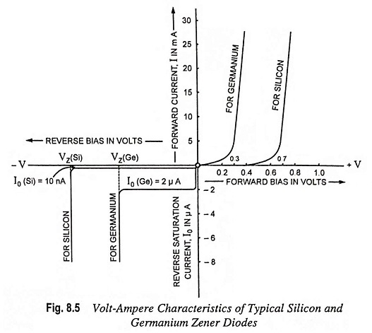
Volt-ampere characteristics of typical silicon and germanium diodes are illustrated in Fig. 8.5. Breakdown diode is operated over the breakdown region and the current is limited by an external resistance. The breakdown or zener voltage VZ depends upon the amount of doping. A heavily doped diode will have very thin depletion layer, so zener voltage will be very low. By controlling the thickness of depletion layer and doping concentration it is possible to make the zener diode to break down at a specified voltage, called the zener voltage (ranging from 2.4 V to 200 V). The forward characteristics of a zener diode are similar to those of an ordinary P-N junction diode, as illustrated.
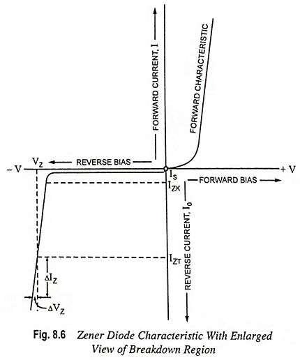
During the operation in the breakdown region, it does not burn out immediately. As long as the current through the diode is limited by the external circuit within permissible values, it does not burn out.
Zener Impedance:
This is very important parameter in the construction and working of zener diode. Zener impedance ZZ is essentially the dynamic resistance of a zener diode (similar to dynamic resistance of an ordinary P-N diode). It is defined as the reciprocal of the slope of the zener curve
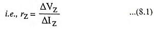
where ΔVZ and ΔIZ are the small variations in voltage and current respectively.
It is usually measured just above the knee in zener region and is named as ZZK. When measured at test point, it is designated ZZT. It decreases with increase in zener current. For this reason, the diode should he operated with as much reverse current as possible, consistent with rating limitations.
Small value of zener impedance is usually desirable as it indicates steep curve where relatively large change in current, ΔIZ occurs with a small change in voltage ΔVZ.
Ideally the breakdown curve should be a perfect vertical line and rZ should be zero. In practice, however, rZ has a small value ranging from a few ohms to several hundred ohms. There is also a variation in impedance of zener diodes among those having different values of VZ. Zener diodes with breakdown voltage near 7 V have the smallest impedances.
Equivalent Circuit of Zener Diode:
Circuit symbol and the equivalent circuit of a zener diode are given in Fig. 8.7. The complete equivalent circuit of a zener diode in the zener region includes a small dynamic resistance rZ and a battery of VZ volts, as illustrated in Fig. 8.7 (b).
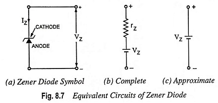
Assuming that breakdown curve is a perfect vertical line i.e., zener dynamic resistance is negligible in comparison to external resistance, the equivalent circuit becomes as illustrated in Fig. 8.7 (c) i.e., it appears like a dc battery of VZ volts.
Temperature Effects:
The breakdown voltage of a zener diode is a function of the width of its depletion region, which is controlled during manufacturing by the degree of impurity doping. As discussed earlier, the mechanism by which breakdown occurs depends on the breakdown voltage itself. For VZ less than 5 V, the high electric field intensity across narrow depletion region (about 3 x 10⁷ V/ m) strips carriers directly from their bonds, a phenomenon usually known as zener breakdown. For VZ exceeding 8 V, breakdown occurs as a result of collision between high-energy carriers, the mechanism known as avalanching. Between 5 V and 8 V, both the avalanching and zener mechanisms contribute to breakdown. The practical significance of these facts is that the breakdown mechanism determines how temperature variations affect the value of zener voltage VZ. Low-voltage zener diodes that break down by zener mechanism have negative temperature coefficient i.e., VZ decreases with the increase in temperature. Higher-voltage avalanche zeners have positive temperature coefficients.
The effect of temperature on zener voltage is given in terms of temperature coefficient, which is defined as the percentage change in nominal zener voltage for each degree Celsius of change in junction temperature. Mathematically it is given as

where ΔVZ is the change in zener voltage due to temperature variation of (t – t0). The zener coefficient may be positive or negative, depending on current, becoming more positive with the increase in current.
Zener Diode Specifications:
Construction and working of zener diode is specified by its breakdown voltage VZ, breakdown current, IZK, the maximum power dissipation PZ(max) and zener impedance measured at test point, ZZT.
Zener diodes are available for zener voltages of 2.4 to 200 V with accuracies between 5 and 20%. The preferred values are 3.3, 4.7, 5.1, 6.1, 9.1, 10, 11, 12, 13, 15, to 200 V.
Power dissipation is the product of VZ and IZ. The maximum power rating varies from 150 mW to 250 W. Commonly available power ratings are 0.4, 1, 3, 10, and 50 watts.