What is Extrinsic Semiconductor?
Intrinsic (or pure) semiconductor by itself is of little significance as it has little current conduction capability at ordinary room temperature. However, the electrical conductivity of intrinsic semiconductor can be increased many times by adding very small amount of impurity (of the order of one atom per million atoms of pure semiconductor) to it in the process of crystallization. This process is called doping and the doped material is called the impurity or extrinsic semiconductor.
Germanium and silicon are tetravalent. So the impurity or doping material may be either pentavalent or trivalent. Accordingly the impurity introduced may be of two types viz. (i) donor type or N-type and (ii) acceptor type or P-type.
Depending on the type of impurity added, the extrinsic semiconductors can be divided into two classes namely (i) N-type semiconductors and (ii) P-type semiconductors.
N-Type Extrinsic Semiconductor:
When a small amount of pentavalent impurity, such as arsenic, antimony, bismuth or phosphorus, is added to a pure semiconductor crystal during the crystal growth, the resulting crystal is called the N-type extrinsic semiconductor, where N stands for negative.
When a pentavalent or a donor impurity is added to silicon (or germanium), the impurity atoms form covalent bonds with the silicon (or germanium) atoms; but since intrinsic semiconductor atoms have only four electrons and four holes in their valence shells, one spare valence-shell electron is produced for each impurity atom added. Each spare electron so produced enters the conduction band of pure semiconductor as a free electron. The pentavalent impurity is called the donor type impurity as it donates one electron to the conduction band of a pure semiconductor. Though each impurity provides only one free electron yet an extremely small amount of impurity provides enough atoms to supply millions of free electrons.
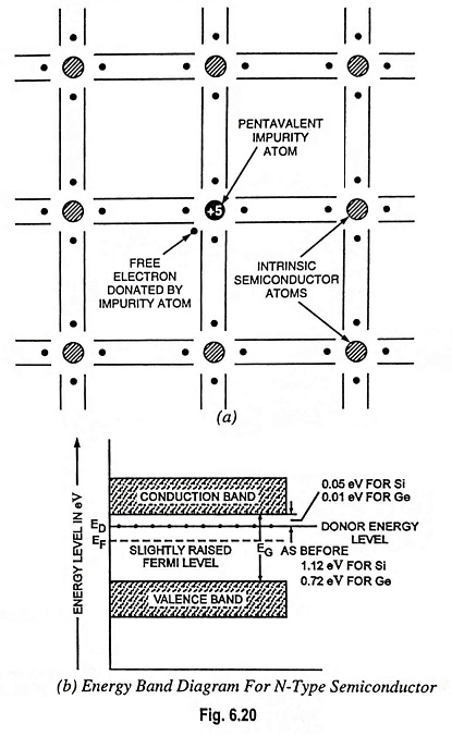
The effect of adding donor impurity in a semiconductor is illustrated in Fig. 6.20 (a). As shown in the figure, the unbound electron remains near its parent atom. This occurs because the impurity atom has a proton in its nucleus which attracts the unbound electron. However, due to the geometry involved, the electron is partially shielded from its parent atom and the attractive force between them is somewhat reduced. The energy required to detach this fifth electron from the atom is of the order of only 0.05 eV for silicon (0.01 eV for germanium). This energy is so small that at room temperature practically all such electrons become free. In other words, at room temperature each impurity atom donates one electron to the conduction band. These donated electrons are called excess electrons, because they are in excess to the electrons which are thermally generated by breaking covalent bonds. However, the number of thermally generated electron-hole pairs will be very small in comparison to the number of free electrons due to the impurity atoms. The effect of this doping process on the relative conductivity can best be explained by energy band diagram shown in Fig. 6.20 (b). When donor impurities are added to an intrinsic semiconductor, allowable energy levels are introduced at a very small distance below the conduction band, as illustrated in Fig. 6.20 (b). These new allowable levels are essentially a discrete level because the added impurity atoms are far apart in the crystal structure and hence their interaction is small. In the case of silicon, the distance of the new discrete allowable energy level is only 0.05 eV (0.01 eV in germanium) below the conduction band and, therefore, at room temperature almost all of the “fifth” electrons of the donor impurity are raised into the conduction band and the conductivity of the material increases considerably. At room temperature in an intrinsic silicon there is about 1 free electron for every 1012 atoms (1 to 109 for germanium). If the dosage level were 1 in 10 million (107), the ratio 1012/107 i.e., 105 would indicate that the carrier concentration has increased by a ratio 105: 1.
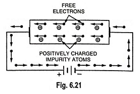
Negative or N-Type Conductivity: When an electric field is applied, the excess electrons donated by impurity atoms move towards the positive terminal of the battery, as shown in Fig. 6.21. This constitutes the electric current. This type of conductivity is called the negative or N-type conductivity because the current flows through the crystal due to free electrons (negatively charged particles)
Although N-type semiconductor has excess of electrons but it is electrically neutral. This is due to the fact that electrons are created by the addition of neutral pentavalent impurity atoms to the pure semiconductor i.e., there is no addition of either negative charges or positive charges.
Since pentavalent impurity donates electrons, which have negative charge, to the pure semiconductor, such an impurity is also called the N-type impurity.
Since current flowing through the crystal is primarily due to free electrons (negatively charged particles), such a conductor is called the N-type semiconductor.
In an N-type semiconductor material, the number of holes is small in comparison to parent intrinsic semiconductor because the larger number of electrons present increase the rate of recombination of electrons with the holes. Thus, the number of free electrons becomes far greater than the number of holes. That is why it is said that an N-type semiconductor has electrons as majority carriers, and the holes as minority carriers.
P-Type Extrinsic Semiconductor:
When a small amount of trivalent impurity, such as boron, galliun, indium or aluminium, is added to a pure semiconductor crystal during the crystal growth, the resulting crystal is called the P-type extrinsic semiconductor, where P stands for positive. The effect of adding one of these impurities in Si or Ge is illustrated in Fig. 6.22.
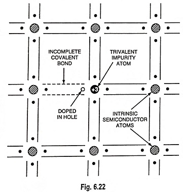
When a trivalent impurity is added to silicon (or germanium), these impurity atoms form covalent bonds with four surrounding intrinsic semiconductor (silicon or germanium) atoms but one bond is left incomplete and gives rise to a hole, as illustrated in Fig. 6.22. Such impurities make available positive carriers because they create holes which can accept electrons. These impurities are consequently known as acceptor or P-type impurities. The amount of impurity which is required to be added to have an appreciable effect on the conductivity is very small.
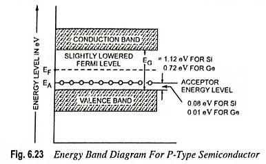
The effect of this doping process on the relative conductivity can best be explained by energy band diagram shown in Fig. 6.23. When acceptor or P-type impurities are added to the intrinsic semiconductor, they produce an allowable discrete energy level which is just above the valence band, as shown in Fig. 6.23. Since a very small amount of energy (0.08 eV in case of silicon and 0.01 eV in case of germanium) is required for an electron to leave the valence band and occupy the acceptor energy level, holes are created in the valence band by these electrons.
The holes so created constitute the larger number of carriers in the semiconductor material.
Since holes can be said to have a positive charge, acceptor-doped semiconductor material is referred to as P-type semiconductor. The resulting P-type material is electrically neutral, for the same reasons as for the N-type material.
The noteworthy points about P-type semiconductors are :
- In P-type semiconductors, the majority carriers are holes while the minority carriers are electrons.
- P-type semiconductor remains electrically neutral as the number of mobile holes under all conditions remains equal to the number of acceptors.
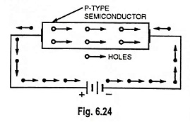
- When an electric field is applied across a P-type semiconductor, as shown in Fig. 6.24, the current conduction is primarily due to holes. Here the holes are shifted from one covalent bond to another covalent bond. As the holes are positively charged, they are directed towards the negative terminal and constitute the hole The hole current flows more slowly than electron current in N-type semiconductor.
- In P-type conductors, the valence electrons move from one covalent bond to another covalent bond unlike N-type where current conduction is by free electrons.
Since the current flowing through the crystal is primarily due to holes, which have positive charge, such a semiconductor is called the P-type semiconductor and the conductivity is called the P-type conductivity. The impurity making P-type semiconductor is also called the P-type impurity.
Note: In the manufacturing process of an extrinsic semiconductor, before doping a pure crystal of silicon or germanium is produced. Then by controlling the amount of impurity, the properties of the semiconductor can be precisely controlled. Historically, pure germanium crystals were easier to produce than pure silicon crystals. This is why the earliest semiconductor devices were made of germanium. Eventually, manufacturing techniques improved and pure silicon crystals became available. Because of its advantages, silicon has become the most popular and useful semiconductor material.
Terms Used in Extrinsic Semiconductors:
Various terms used in reference to extrinsic semiconductors are explained below.
- Doping. Addition of impurity atoms to intrinsic semiconductor crystal is called the doping and the impurity used for doping is called the dopant.
- Diffusion. The process of doping a semiconductor with impurities is known as diffusion.
- Donor. Arsenic, antimony or phosphorus or any other pentavalent impurity used as dopant to produce an N-type semiconductor is called the donor type impurity.
- Acceptor. Boron, gallium, indium or any other trivalent impurity used as dopant to produce a P-type semiconductor is called the acceptor type impurity.
Effect of Temperature on Extrinsic Semiconductors:
Addition of a small amount of impurity (donor or acceptor) produces a large number of charge carriers in an extrinsic semiconductor, as already discussed above. In fact, this number is so large that the conductivity of an extrinsic semiconductor is many times that of an intrinsic semiconductor at room temperature.
If the temperature of an extrinsic semiconductor (say N-type) is raised, the additional thermal energy increases the thermally generated carriers. As a result, the concentration of minority carriers increases. Eventually, a temperature is reached, called the critical temperature, (85°C in case of Ge and 200°C in case of Si) when the number of covalent bonds, that are broken is very large, so that the number of holes becomes approximately the same as the number of electrons. The extrinsic semiconductor now behaves like an intrinsic semiconductor but with higher conductivity.
Charge Carriers:
As discussed above, current conduction in an N-type semiconductor is due to excess of free electrons whereas in a P-type semiconductor it is due to excess of holes. One may think that N-type semiconductor has a net negative charge and P-type has a net positive charge. But this conclusion is wrong. Even though the N-type semiconductor has excess free electrons but these extra electrons were supplied by the atoms of donor impurity and each atom of donor impurity is electrically neutral. When the donor impurity is added, the term “excess electrons” refers to the excess with reference to the number of electrons required to fill the covalent bonds in the semiconductor crystal. The extra free electrons are there to increase the conductivity of the semiconductor, however, N-type semiconductor is electrically neutral. Similar situation occurs in P-type semiconductor which is also electrically neutral. Free electrons in N-type semiconductors and holes in P-type semiconductors are charge carriers.
Majority and Minority Charge Carriers:
In the intrinsic state, the number of free electrons in silicon or germanium is due only to those few electrons in the valence band that have acquired sufficient energy from heat or light sources to break the covalent bond or to the few impurities that could not be removed. The vacancies left behind in the covalent bonding structure represent very limited supply of holes. In an N-type material, the number of holes has not changed significantly from this intrinsic level and the number of electrons (both added and thermally generated) far outweighs the number of thermally generated holes. Hence in an N-type material electrons are majority carriers and responsible for flow of current.
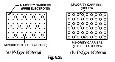
The reverse is true for the P-type material i.e., P-type materials have holes as majority carriers and free electrons as minority carriers, as illustrated in Fig. 6.25 (b).