Zener Diodes Characteristics:
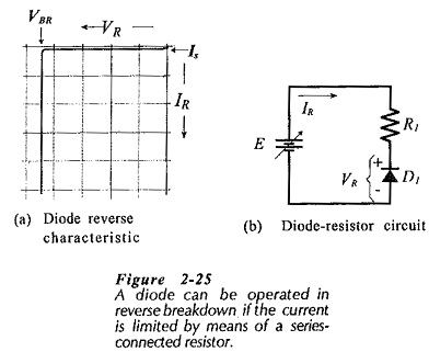
When a Junction diode is reverse biased, normally only a very small reverse saturation current flows; IS on the reverse characteristic in Fig. 2-25(a). When the reverse voltage is sufficiently increased, the junction breaks down and a large reverse current flows. If the reverse current is limited by means of a suitable series resistor, [R1 in the circuit in Fig. 2-25(b)], the power dissipation in the junction can be kept to a level that will not destroy the device. In this case, the Zener Diodes Characteristics may be operated continuously in reverse breakdown. The reverse current returns to its normal level when the voltage is reduced below the reverse breakdown level.
Diodes designed for operation in reverse breakdown are found to have a breakdown voltage that remains extremely stable over a wide range of current levels. This property gives the breakdown diode many useful applications as a voltage reference source.
There are two mechanisms that cause breakdown in a reverse biased pn- junction. With a very narrow depletion region, the electric field strength (volts/width) produced by a reverse bias voltage can be very high. The high intensity electric field causes electrons to break away from their atoms, thus converting the depletion region from an insulating material into a conductor. This is ionization by electric field, also called Zener breakdown, and it usually occurs with reverse bias voltages less than 5 V.
In cases where the depletion region is too wide for Zener breakdown, the electrons in the reverse saturation current can be given sufficient energy to cause other electrons to break free when they strike atoms within the depletion region. This is termed ionization by collision. The electrons released in this way collide with other atoms to produce more free electrons in an avalanche effect. Avalanche breakdown is normally produced by reverse voltage levels above 5 V. Although Zener and avalanche are two different types of breakdown, the name Zener Diodes Characteristics is commonly applied to all breakdown diodes.
Circuit Symbol and Package:
The circuit symbol for a Zener Diodes Characteristics in Fig. 2-26(a) is the same as that for an ordinary diode, but with the cathode bar approximately in the shape of a letter Z. The arrowhead on the symbol still points in the (conventional) direction of forward current when the device is forward biased. As illustrated, for operation in reverse bias, the voltage drop (VZ) is + on the cathode, – on the anode.
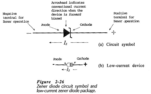
Low-power Zener diodes are available in a variety of packages. For the device package shown in Fig. 2-26(b), the colored band identifies the cathode terminal, as in the case of an ordinary low-current diode. High-current Zener diodes are also available in the type of package that allows for mounting on a heat sink.
Characteristics and Parameters:
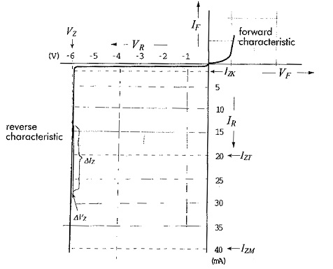
The typical Zener Diodes Characteristics are shown in detail in Fig. 2-27. Note that the forward characteristic is simply that of an ordinary forward-biased diode. Some important points on the reverse characteristic are:
VZ – Zener breakdown voltage
IZT – Test current for measuring VZ
IZK – Reverse current near the knee of the characteristic; the minimum reverse current to sustain breakdown
IZM – Maximum Zener current; limited by the maximum power dissipation.
The dynamic impedance (ZZ) is another important parameter that may be derived from the characteristics. As illustrated in Fig. 2-27, ; ZZ defines how VZ changes with variations in diode reverse current. When measured at IZT, the dynamic impedance is designated (ZZT). The dynamic impedance measured at the knee of the characteristic (ZZK) is substantially larger than ZZT.
The Zener diode current may be any level between IZK and IZM. For greatest voltage stability, the diode is normally operated at the test current. Many low-power Zener diodes have a test current specified as 20 mA, however, some devices have lower test currents.
Data Sheet:
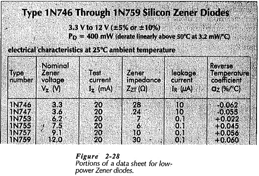
Portions of a data sheet for low-power Zener diodes with voltages ranging from 3.3 V to 12 V is shown in Fig. 2-28. (A data sheet for 2.4 V to 110 V Zener diodes. Note in Fig. 2-28 that the VZ tolerance is ±5% or ±10%. This means, for example, that for a 1N753 with a ±10% tolerance the actual VZ level is 6.3 V ±10%, or 5.67 V to 6.93 V. The Zener voltage remains stable at whatever it happens to be within this range.
The data sheet also lists the dynamic impedance, reverse leakage current, and the temperature coefficient for the VZ of each device. The Zener voltages at any temperature can be calculated from,
![]()
Temperature compensated Zener Diodes Characteristics are also available with extremely low temperature coefficients.
Low-power Zener diodes are typically limited to a maximum power dissipation of 400 mW, (PD in F’g. 2-28). Higher-power devices are available. All of the power dissipation must be derated with temperature increase. When the maximum Zener current is not listed on the device data sheet, it may be calculated from the power dissipation equation.
![]()
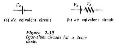
Equivalent Circuit:
The dc equivalent circuit for a Zener diode is simply a voltage cell with a voltage VZ, as in Fig. 2-30(a). This is the complete equivalent circuit for the device for all dc calculations. For the ac equivalent circuit [Fig. 2-30(b)I, the dynamic impedance is included in series with the voltages cell. The ac equivalent circuit is used in situations where the Zener current is varied by small amounts. It must be understood that these equivalent circuits apply only when the Zener diode is maintained in reverse breakdown. If the device becomes forward biased, then the equivalent circuit for a forward-biased diode must be used.