Pulsed Radar System Block Diagram:
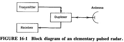
A very Pulsed Radar System Block Diagram set was shown in Figure 16-1. A more detailed block diagram will now be given, and it will then be possible to compare some of the circuits used with those treated in other contexts and to discuss in detail those circuits peculiar to radar.
Block diagram and description:
The block diagram of Figure 16-4 shows the arrangement of a typical high-power Pulsed Radar System Block Diagram. The trigger source provides pulses for the modulator. The modulator provides rectangular voltage pulses used as the supply voltage for the output tube, switching it ON and OFF as required. This tube may be a magnetron oscillator or an amplifier such as the klystron, traveling-wave tube or crossed-field amplifier, depending on specific requirements. If an amplifier is used, a source of microwaves is also required. While an amplifier may be modulated at a special grid, the magnetron cannot. If the radar is a low-powered one, it may use IMPATT or Gunn oscillators, or TRAPATT amplifiers. Below C band, power transistor amplifiers or oscillators may also be used. Finally, the transmitter portion of the radar is terminated with the duplexer, which passes the output pulse to the antenna for transmission.
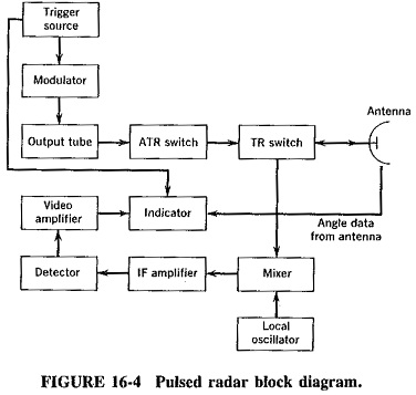
The receiver is connected to the antenna at suitable times in the Pulsed Radar System Block Diagram (i.e., when no transmission is instantaneously taking place). As previously explained, this is also done by the duplexer. As shown here, a (semiconductor diode) mixer is the most likely first stage in the receiver, since it has a fairly low noise figure, but of course it shows a conversion loss. An RF amplifier can also be used, and this would most likely be a transistor or IC, or perhaps a tunnel diode or paramp. A better noise figure is thus obtained, and the RF amplifier may have the further advantage of saturating for large signals, thus acting as a limiter that prevents mixer diode burnout from strong echoes produced by nearby targets. The main receiver gain is provided at an intermediate frequency that is typically 30 or 60 MHz. However, it may take two or more down-conversions to reach that IF from the initial microwave RF, to ensure adequate image frequency suppression.
If a diode mixer is the first stage, the (first) IF amplifier must be designed as a low-noise stage to ensure that the overall noise figure of the receiver does not deteriorate. A noisy IF amplifier would play havoc with the overall receiver performance, especially when it is noted that the “gain” of a diode mixer is in fact a conversion loss, typically 4 to 7 dB. A cascode connection is quite common for the transistor amplifiers used in the IF stage, because it removes the need for Neutralization to avoid the Miller effect.
Another source of noise in the receiver of Figure 16-4 may be the local oscillator, especially for microwave radar receivers. One of the methods of reducing such noise is to use a varactor or step-recovery diode multiplier. Another method involves the connection of a narrowband filter between the local oscillator and the mixer to reduce the noise bandwidth of the mixer. However, in receivers employing automatic frequency correction this may be unsatisfactory. The solution of the oscillator noise problem may then lie in using a balanced mixer and/or a cavity-stabilized oscillator. If used, AFC may simply consist of a phase discriminator which takes part of the output from the IF amplifier and produces a dc correcting voltage if the intermediate frequency drifts. The voltage may then be applied directly to a varactor in a diode oscillator cavity.
The IF amplifier is broadband, to permit the use of fairly narrow pulses. This means that cascaded rather than single-stage amplifiers are used. These can be synchronous, that is, all tuned to the same frequency and having identical bandpass characteristics. If a really large bandwidth is needed, the individual IF amplifiers may be stagger-tuned. The overall response is achieved by overlapping the responses of the individual amplifiers, which are tuned to nearby frequencies on either side of the center frequency. The detector is often a Schottky-barrier diode, whose output is amplified by a video amplifier having the same bandwidth as the IF amplifier. Its output is then fed to a display unit, directly or via computer processing and enhancing.
Modulators:
In a Pulsed Radar System Block Diagram transmitter, the modulator is a circuit or group of circuits whose function it is to switch the output tube ON and OFF as required. There are two main types in common use: Line-Pulsing Modulators and Active-Switch Modulators. The latter are also known as Driver-Power-Amplifier Modulators and were called Hard-Tube Modulators until the advent of semiconductor devices capable of handling some modulator duties.
The line-pulsing modulator corresponds broadly to the high-level modulator. Here the anode of the output tube (or its collector, depending on the tube used) is modulated directly by a system that generates and provides large pulses of supply voltage. This is achieved by slowly charging and then rapidly discharging a transmission line. The charging is made slow to reduce the current requirements and is generally done through an inductance. The transmission line is able to store energy in its distributed inductance and capacitance. If the line is charged to a voltage V from a high-impedance source, this voltage will drop to 1/2V when a load is connected (the output tube) whose impedance is equal to the characteristic impedance of the line. However, at the instant of load connection the voltage across the line is 1/2V only at the input; it is still V everywhere else. The voltage drop now propagates along the line to the far end, from which it is reflected to the input terminals. It is thus seen that a voltage 1/2V will be maintained across the load for a time 2t, where t is the time taken by an electromagnetic wave to travel from one end of the line to the other.
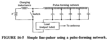
If the pulse duration (2t) is to be 1 μs, the line length must be 150 m. This is far too long for convenience, and consequently a Pulse Forming Network (PFN) is almost always substituted for the transmission line. As shown in Figure 16-5, which illustrates a very basic modulator, the PFN looks just like the equivalent circuit of a transmission line. It also behaves identically to the transmission line for frequencies below f = 1/π√LC, where L and C are the inductance and capacitance, respectively, per section. In high-power radars, the device most likely for use as a switch is a hydrogen thyratron, because it is capable of switching very high powers and of rapid deionization. Silicon-Controlled Rectifiers (SCRs) may also be used to good advantage.
The advantages of the line modulator are that it is simple, compact, reliable and efficient. However, it has the disadvantage that the PFN must be changed if a different pulse length is required. Consequently, line modulators are not used at all in radars from which variable pulse widths are required, but they are often used otherwise. The Pulsed Radar System Block Diagram that are produced have adequately steep sides and flat tops.
The active-switch modulator is one that can also provide high-level modulation of the output tube, but this time the pulses are generated at a low power level and then amplified. The driver is often a blocking oscillator, triggered by a timing source and driving an amplifier. Depending on the power level, this may be a transistor amplifier or a powerful tube such as a shielded-grid triode. The amplifier then controls the dc power supply for the output RF tube. This type of modulator is less efficient, more complex and bulkier than the line modulator, but it does have the advantage of easily variable pulse length, repetition rate or even shape. It is often used in practice.
Finally, low-level modulation is also sometimes possible. This may be done in UHF radar, which uses orthodox vacuum tubes, or at higher frequencies if a velocity-modulated amplifier is used.