Memory Addressing Modes of 8086:
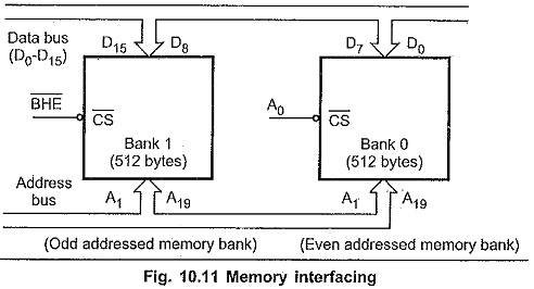
Most of the memory ICs are byte oriented i.e. each memory location can store only one byte of data. The 8086 is a 16-bit microprocessor, it can transfer 16-bit data. So in addition to byte, word (16-bit) has to be stored in the memory. This is stored by using two consecutive memory locations, one for least significant byte and other for most significant byte. The Memory Addressing Modes of 8086 of word is the address of least significant byte. To implement this, the entire memory is divided into two memory banks : bank0 and bank1. Fig. 10.11 shows the interfacing diagram to these memory banks. Bank0 is selected only when A0 is zero and Bank1 is selected only when BHE is zero. A0 is zero for all even addresses. So Bank0 is usually referred as even addressed memory bank. BHE is used to access higher order memory bank, referred to as odd addressed memory bank.
Together BHE and A0 tell the interface how the data appears on bus. Four possible combinations are shown in the Table 10.2.
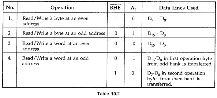
Note : To access odd addressed word two bus cycles are required.
Every microprocessor based system has a memory system. Almost all systems contain two basic types of memory, read-only memory (ROM) and random access memory (RAM) or read/write memory. Read only memory contains system software and permanent system data such as lookup tables, while Random Access Memory contains temporary data and application software. ROMs / PROMs / EPROMs are mapped to cover the CPU’s reset address, since these are non-volatile. When the 8086 is reset; the next instruction is fetched from memory location FFFF0H. So in the 8086 systems, the location FFFF0H must be ROM location.
The 8086 microprocessor provides 20-bit Memory Addressing Modes of 8086 that allows up to 1 Mbyte main memory. It is important in any memory interface that one block of memory must not be allowed to overlap another memory block. So in order to connect a memory device to the microprocessor, it is necessary to decode the address from the microprocessor to access each memory IC independently.