Partial Discharge Measurements:
Earlier the testing of insulators and other equipment was based on the insulation resistance measurements, dissipation factor measurements and breakdown tests. It was observed that the dissipation factor (tan δ) was voltage dependent and hence became a criterion for the monitoring of the high voltage insulation. In further investigations it was found that weak points in an insulation like voids, cracks, and other imperfections lead to internal or intermittent discharges in the insulation. These imperfections being small were not revealed in capacitance measurements but were revealed as power loss components in contributing for an increase in the dissipation factor. In modern terminology these are designated as “Partial Discharge Measurements” which in course of time reduce the strength of insulation leading to a total or partial failure or breakdown of the insulation.
If the sites of Partial Discharge Measurements can be located inside an equipment, like in a power cable or a transformer, it gives valuable information to the insulation engineer about the regions of greater stress and imperfections in the fabrication.
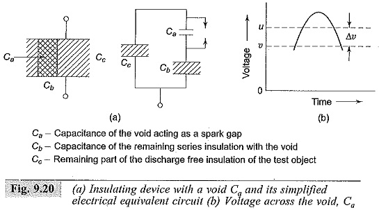
Electrical insulation with imperfections or voids leading to Partial Discharge Measurements can be represented by an electrical equivalent circuit shown in Fig. 9.20. Consider a capacitor with a void inside the insulation (Ca). The capacitance of the void is represented by a capacitor in series with the rest of the insulation capacitance (Cb). The remaining void-free material is represented by the capacitance Cc. When the voltage across the capacitor is raised, a critical value is reached across the capacitor Ca and a discharge occurs through the capacitor, i.e. it becomes short circuited. This is represented by the closure of the switch.
Generally Ca << Cb << Cc. A charge Aga which was present in the capacitor Ca flows through Cb and Cc giving rise to a voltage pulse across the capacitor Cc. A measure of the voltage pulse across the capacitor gives the amount of discharge quality. But this measurement is difficult in practice, and an apparent charge measurement across a detecting impedance is usually made.
Discharge Detection Using Straight Detectors:
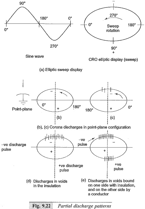
The circuit arrangement shown in Fig. 9.21 gives a simplified circuit for detecting “partial discharges“. The high voltage transformer shown is free from internal discharges. A resonant filter is used to prevent any pulses starting from the capacitance of the windings and bushings of the transformer. Cx is the test object, Cc is the coupling capacitor, and Zm is a detection impedance. The signal developed across the impedance Z is passed through a band pass filter and amplifier and displayed on a CRO or counted by a pulse counter multi-channel analyzer unit.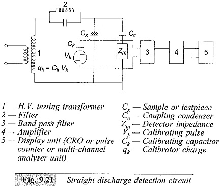 In Fig. 9.22, the discharge pattern displayed on the CRO screen of a Partial Discharge Measurements detector with an elliptical display is shown. The sinusoidal voltage and the corresponding ellipse pattern of the discharge are shown in Fig. 9.22a and a single corona pulse in a point-plane spark gap geometry is shown in Figs 9.22b and c. When the voltage applied is greater than that of the critical inception voltage, multiple pulses appear (see Fig. 9.22c), and all the pulses are of equal magnitude. A typical discharge pattern in cavities inside the insulation is shown in Fig. 9.22d. This pattern of discharge appears on the quadrants of the ellipse which correspond to the test voltage rising from zero to the maximum, either positively or negatively. The discharges usually start near the peaks of the test voltage but spread towards the zero value as the test voltage is increased beyond the inception level. The number and magnitude of the discharges on both the positive and negative cycles are approximately the same. A typical discharge pattern from a void bounded on one side by the insulation and the other side by a conductor is shown in Fig. 9.22c. This pattern of discharge is common in insulated cables (like polyethylene and XLPE cables) when the discharge is made up of a large number of pulses of small magnitude on the positive cycle and a much smaller number of large magnitude pulses on the negative half-cycle.
In the narrow band detection scheme Zm is a parallel L-C circuit tuned to 500 kHz. The bandpass filter has a bandwidth of about ± 10 kHz. The pulses after amplification are displayed in an elliptical time base of a CRO, and the resolution for the pulses is about 35 per quadrant.
In the wide band detection scheme Zm is an R-C network connected to a double tuned transformer. The bandwidth is about 250 kHz with centre frequency between 150 and 200 kHz. A wide band amplifier is used, and the signal is displayed on the CRO as in the previous case. The resolution is about 200 pulses per quadrant.
With tuned narrow band detectors, the Partial Discharge Measurements can be detected with a sensitivity less than one pico coulomb for a testpiece capacitance of 100 pF. Testpieces with capacitances in the range 100 pF to 0.1 pF can be tested. With the wide band detector samples up to 250 μF capacitance can be tested. Sensitivity of the measurement varies from 0.005 pico coulomb at 6 pF sample capacitance to about 15 pc at a sample capacitance of 250 μF.
Balanced Detection Method:
In the straight detection method, the external disturbances are not fully rejected. The filter used to block the noise sources may not be effective. The Schering bridge employed for the tan δ measurement is sometimes used. In this method, the test object is not grounded. A modification to the Schering bridge detector is the differential discharge detector, given by Kreuger. Both the schemes are given in Fig. 9.23.
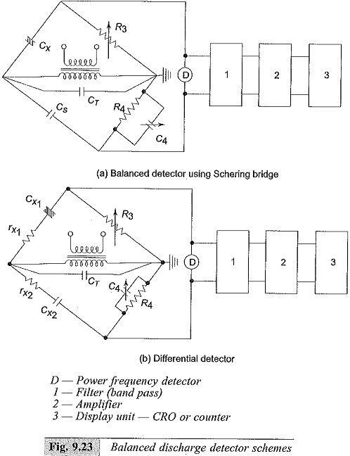
The bridges are tuned and balanced at 50 Hz. A filter is used across the detector terminals to block the 50 Hz components present. Signals in the range from 5 to 50 kHz are allowed to pass through the filter and amplified. The CRO gives the display of the pulse pattern. Any external interference from outside is balanced out, and only internally (testpiece) generated pulses are detected. In the modified scheme, another test sample called dummy sample is used in the place of the standard capacitor. The capacitance and tan δ of the dummy sample are made approximately equal, but need not be equal. The disadvantage is that if two discharges occur in both the samples simultaneously, they cancel out, but this is very rare. The main advantage of the second method is its capacity for better rejection of external noise and use of the wide frequency band with better resolution of the individual pulses.
Calibration of Discharge Detectors:
Partial Discharge Measurements are connected across a measuring impedance Zm as shown in Fig. 9.21 and the signal measured across this impedance is read by the detector. The signal voltage developed across Zm depends on the circuit parameters Cx and Cc and also on the internal circuitry of the instrument (blocks 3, 4, 5 shown in Fig. 9.21).
Hence, the measuring instrument or detector is calibrated by injecting a pulse having a charge of known magnitude into the detecting system. For this purpose, a square wave generator and a calibrating capacitor (Ck) are usually used. The magnitude of the charge injected is qk =CkVk, where Vk is the magnitude of the voltage pulse. The rise time of the pulse is about 0.1 μ sec, and the pulse width varies from 10 to 20 μ sec. With suitable attenuation, the output voltage of the pulse generator can be varied from a minimum output of about 10 μV to a maximum value of 100 V in steps. The value of Ck, usually used, lies between 1000 and 2500 pF. If the calibrating pulse is directly injected at the H.V. terminal of the test object, the magnitude of the calibration pulse will be Ck . Vk. If the pulse is injected across the measuring impedance (as shown in Fig. 9.21), then the calibrating pulse magnitude should be multiplied by (Cx + Cc)/Cc.
Another method of calibration is to use a secondary standard, consisting of a point-hemisphere electrode system of specified dimensions.
This method is more accurate and is easily reproducible. With an over voltage of 10 — 20% applied above the discharge inception voltage, the arrangement gives discharges which are used for calibration purposes.
P.D. Measuring and Analysing System:
A modern P.D. measuring system consists of a discharge free source (transformer), filter unit, a coupling capacitance, a test sample or an object and measuring impedance, Zm for different sample capacitances. The output from the measuring unit is fed to the measuring and analysing system consisting of
(i) the p.d. measuring band selector,
(ii) and amplifier
(iii) pulse magnitude counter
(iv) pulse pattern analyser
(v) pulse shape recorder, etc.
All the above units are controlled by a microprocessor based p.c. unit that can make the pulse analysis as desired. All the P.D. quantities are displaced in real time mode if needed. Pulse resolution up to 100 kHz and pulse magnitude detection for less than 1 pC are possible. The software associated is available in Windows NT etc.
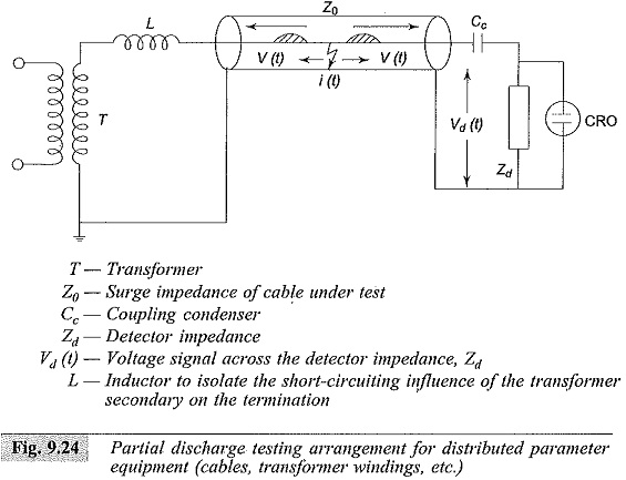
Discharge Detection in Power Cables:
Power cables of great lengths may be considered to be specimens with distributed capacitance rather than a lumped capacitance. The same feature is true for windings of the transformers and rotating machines of high voltage ratings. In such cases, the location of discharge is done using the travelling wave technique, and the circuit for the same is shown in Fig. 9.24. The breakdown or discharge in a cavity at location F causes a charge accumulation at the fault point F. This creates two travelling waves which travel in opposite directions towards the cable ends. The voltage wave is given by

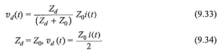
If Cc is neglected in comparison with the detection impedance Zd, the voltage signal across the detection impedance becomes
If the Partial Discharge Measurements site is located exactly in the middle of the cable, the travelling wave moving to the left is reflected without any polarity change at the open end and then arrives at the detection impedance, Zd, separated from the direct pulse by a time equal to the cable transit time τ. If the site is at any other point, the time difference between the original pulse and its reflection may be any value from 0 to 2τ. Usually, the supply transformer end is not strictly an open circuit because of the shunt capacitance of the windings of the transformer. Therefore, the travelling wave is reflected from the transformer end with the surge impedance of the transformer as its termination. To avoid this reflection an inductor is inserted at the transformer end. By knowing the transit time of the cable τ and the actual time difference between the two pulses, the fault position can be located.