Ion Implantation Process in IC Fabrication:
As we know, the conductivity of the semiconductor increases when small impurity is added to it. The process of adding impurity is called doping while the impurity to be added is called dopant. So ion implantation is a process of adding dopant to the silicon substrate. The ion implantation process is controllable, reproducible and also there are no unwanted side effects.
The ion implantation process is prefered over diffusion because of following reasons.
- the impurity concentration is highly uniform typically within 1%, over the wafer,
- the degree of uniformity is maintained same from wafer to wafer,
- the layer can be formed any-where within substrate,
- the lateral spread is very small.
Basically the ion implantation process is low temperature process. In this process, the dopant atoms are vaporised. They are accelerated by an accelerator and then bombarded on silicon substrate. The entire wafer or selected part of it, is exposed to the beam of vaporised, accelerated dopant atoms. The beam injects the dopant atoms into unmasked sections of the substrate. The depant atoms directly enter the crystal lattice of the silicon. In the lattice, due to the collisions with silicon atoms the dopant atoms starts loosing energy. When the energy is totally lost, the dopant atoms are found at some depth within the lattice itself. The depth of penetrations is controlled by the acceleration energy of the incident beam and the doping concentration. In general, the ion implantation is made through thin oxide, as compared to masking which is made through thicker layer of oxide.
The main objective of the basic Ion Implantation Process is to direct a beam of dopant atoms with the appropriate acceleration and energy to the silicon substrate. The schematic diagram of a typical ion-implanter is as shown in the Fig. 1.15.
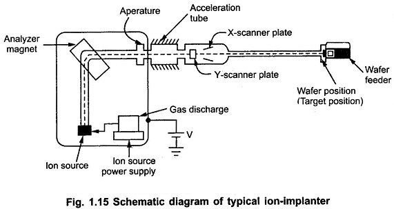
The main blocks of the ion-implanter are ion source, bending analyzer magnet, aperture, acceration tube, X-Y scanner plates, target chamber. There are two distinct parts of the system namely high voltage chamber consisting number of system components producing desired ions, while other one is target chamber consisting wafer holding and feeder assemby.
A gas source delivers a small amount of gas into the ion source. The gas used is BF3. There are molecules break into charged particles due to the heating filament. Now in the ion source, there are desired ions along with other charged particles.
Due to the high voltage (about 20 kV), the charged ions are pulled out of the ion source into the bending magnet analyzer. Note that the pressure in the system is maintained very low (of the order of 10-6 Torr) so as to avoid scattering of ions due to gas molecules. The bending analyzer magnet selects the ions with desired charge to mass ratio with the help of properly applied magnetic field. Thus the desired ions only can travel through the analyzer, while the others impinge on the analyzer walls. In the acceleration tube, the ions are accelerated to the suffeciently high implantation energy.
The aperture focusses the beam of ions. The X-Y scanner plates adjust the sweep of the beam over the wafer placed in target chamber. The wafer is slightly offset to the axis of the acceleration tube so as to avoid deflection of ions on to the wafer. In typical ion-implanter, accelerator voltages range from few kV to 250 kV for medium energy implanters, while upto 2 MV for high energy implanters. Typically a medium energy implanter is 6m long, 3m wide and 2 m high. It process 200 wafers per hour. The total number of ions enetering the target is called dose. The medium energy implantation dosage extends from about 1010 to 1017 atoms/cm2.