Semiconductor

PN Junction Forward Bias

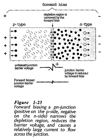
PN Junction Forward Bias: Consider the effect of an external bias voltage applied with the polarity of PN Junction Forward Bias shown in Fig. 1-23; positive on the p-side, negative on the n-side. The holes on the p-side, being positively charged particles, are repelled from the positive terminal and driven toward the junction. Similarly, the […]

PN Junction Forward Bias Read More »

Reverse Bias PN Junction

Reverse Bias PN Junction: When an external bias voltage is applied to a pn-junction, positive to the n-side and negative to the pride, electrons from the n-side are attracted to the positive terminal, and holes from the p-side are attracted to the negative terminal. As shown in Fig. 1-21, holes on the p-side of the

Reverse Bias PN Junction Read More »

PN Junction Semiconductor

PN Junction Semiconductor: Two blocks of PN Junction Semiconductor material are represented in Fig. 1-17; one block is p-type material, and the other is n-type. The small circles in the p-type material represent holes, which are the majority charge carriers in p-type. The dots in the n-type material represent the majority charge carrier free electrons

PN Junction Semiconductor Read More »

P Type and N Type Semiconductor

P Type and N Type Semiconductor: Doping : Pure semiconductor material is known as intrinsic material. Before intrinsic material can be used for device manufacture, impurity atoms must be added to improve its conductivity. The process of adding the atoms is termed doping. Two different types of doping are possible; donor doping, and acceptor doping.

P Type and N Type Semiconductor Read More »

Conductor Semiconductor and Insulator

Conductor Semiconductor and Insulator: Bonding Forces Between Atoms: Whether a material is a Conductor Semiconductor and Insulator depends largely upon what happens to the outer-shell electrons when the atoms bond themselves together to form a solid. In the case of copper, the easily detached valence electrons are given up by the atoms. As illustrated in

Conductor Semiconductor and Insulator Read More »

Conduction in Solids

Conduction in Solids: Conduction in Solids or any given material occurs when an applied voltage causes electrons within the material to move in a desired direction. This may be due to one or both of two processes; Electron Motion and Hole Transfer. In electron motion, free electrons in the Conduction band are moved under the

Conduction in Solids Read More »

Scroll to Top