Zener Diodes Characteristics
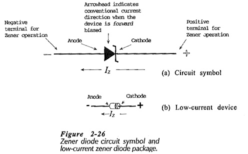
Zener Diodes Characteristics: When a Junction diode is reverse biased, normally only a very small reverse saturation current flows; IS on the reverse characteristic in Fig. 2-25(a). When the reverse voltage is sufficiently increased, the…
Comments Off on Zener Diodes Characteristics
January 29, 2019