Types of Forced Commutation:
It was observed from the discussion on choppers and inverters that in thyristor systems fed from dc supply, the forward current does not pass through zero naturally and must therefore be forced to become zero at appropriate instants by means of auxiliary circuitry, called the commutation circuit. Apart from forcing the forward current to zero, the commutation circuit must also apply a reverse voltage to the thyristor being commutated for sufficient duration (at least equal to its turn-off time) to accelerate and complete the recovery process of the thyristor blocking state. This process of turning off the thyristor as mentioned earlier is called forced commutation.
In general, a forced commutation circuit consists of an oscillatory LC circuit, which can be considered as a voltage or current source in relation to the thyristor. The commutating voltage or current source can be introduced either in series with the thyristor or in parallel across it by means of some auxiliary device. Forced commutation circuits are divided into two general categories:
- Series commutation in which the commutating capacitor is in series with the thyristor to be turned off.
- Parallel commutation in which the commutating capacitor is in parallel with the thyristor to be turned off.
There are various configurations in both these categories. One such parallel commutation configuration was described earlier in connection with the chopper commutation. Rather than giving the detailed configurations of commutation circuits, the basic principles of their operation will be given here.
1. Series Resonance Turn–off:
This types of Forced Commutation is also called load commutation as it depends upon the nature of the load. In the circuit of Fig. 11.58(a) if the thyristor is turned on, it will not turn off naturally because of the continuity of current. To turn off the thyristor a series capacitor is included in the circuit as shown in Fig. 11.58(b) such that the circuit is underdamped. If the load inductance is negligible, a series inductor must be included in the circuit to make it oscillatory. Figure 11.58(c) shows the oscillatory current of the circuit of Fig. 11.58(b) in the absence of the thyristor. At the end of the first positive current pulse, the thyristor current falls to zero and it turns off. In the meantime capacitor C has been charged positively as shown which reverse-biases the thyristor to complete the turn-off process. The current through the thyristor is nearly sinusoidal so that the initial switching current has low di/dt limiting the switching loss.
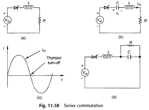
This types of Forced Commutation circuits have been operated successfully at 20 to 30 kHz, the frequency limitation being on account of the thyristor turn-off time which must be less than a quarter-cycle period of the circuit oscillation. One disadvantage of this type of commutation is that the load regulation is poor.
Figure 11.58(d) shows an alternative configuration of the series commutation circuit. Here the circuit oscillation will cause C to charge to a voltage nearly twice the supply voltage (i.e., 2 Vdc). The turn off is obviously accomplished in shorter time here.
2. Parallel Resonance Turn-off:
Figure 11.59 illustrates the principle of parallel commutation. When the thyristor is off, C charges to Vdc as shown. As the thyristor is turned on, it conducts the load current IR and the oscillatory current of the LC circuit. The current in the LC circuit reverses in the second-half oscillation (see Fig. 11.58(c)). This reduces the thyristor current to zero switching it off. The charge still remaining on C reverse-biases the thyristor after current zero.
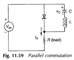
The advantages of this types of Forced Commutation are good load regulation and that the voltage across the thyristor is restricted to no more than the supply voltage. If load resistance R is increased, the charging of capacitor C will be slow, making the minimum off-time longer. Hence this circuit is mostly restricted to loads of constant resistance.
3. Complementary Commutation:
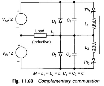
Figure 11.60 shows the circuit of a single-phase half-bridge inverter with the inclusion of commutating capacitors C1 and C2 and indictors L1 and L2 which are tightly coupled. This circuit provides for complementary impulse voltage commutation. In this circuit if Th1 is on, firing Th2 automatically transfers the load current to Th2, turning Th1 off. The load being assumed inductive implies that the load current I0 is almost steady. When Th1 is conducting, the voltage drop across L1 is negligible as the rate of change of the inductive load current is small. Capacitance C2 therefore charges to Vdc, the supply voltage. The energy stored in the magnetic field of the inductor is 1/2 LI02, I0 being the load current. The circuit model prior to triggering Th2 is shown in Fig. 11.61(a).
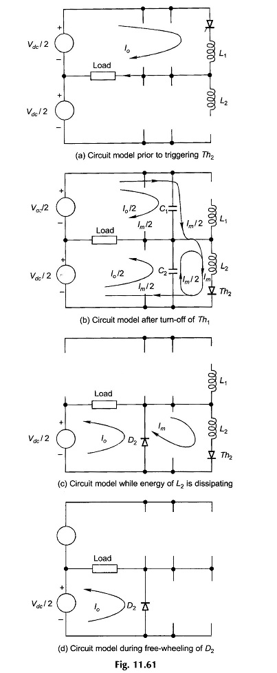
As Th2 is fired, the voltage Vdc of C2 appears across L2 ; as a consequence, voltage Vdc is induced across L1 which reverse-biases Th1 and turns it off. This interrupts the current I0 in L1 which gets immediately transferred to L2 since the magnetic flux cannot change instantly. Further, since the inductive load current cannot get interrupted, it is fed equally (I0/2) by capacitors C1 and C2; C1 is getting charged and C2 is getting discharged at the same rate. The capacitor C2 is now placed in parallel with L2 (as Th2 is turned on) and an oscillatory current appears in the closed loop. At the first quarter-cycle of this oscillation, the oscillatory current rises to its maximum value Im. At this instant Th2 is carrying Im which returns equally via the two capacitors. Thus current in both C1 and C2 is (I0 + Im)/2 as shown in the circuit model of Fig. 11.61(b).
In the process C1 is charging to the supply voltage while the induced voltage across L1 is reducing. This causes Th1 to become forward-biased. At the end of the charging process as C1 gets charged to Vdc, the voltage across C2 simultaneously
reduces to zero. As C2 tends to become oppositely charged during the second quarter of the oscillatory current, the diode D2 goes into the conducting mode and the current (I0 + Im) immediately transfers to it. The current Im flowing in L2 and its associated energy dissipates through Th2 and D2 at the end of which Th2 turns off. This dissipation mode is shown in the circuit model of Fig. 11.61(c). The inclusion of a small resistance in series with the diode would speed up the dissipation process.
The capacitor C1 has by now been fully charged to Vdc and the load current I0 is being fed by D2 as shown in the circuit model of Fig. 11.61(d). After I0 has decayed to zero via the free-wheeling diode D2, D2 blocks off and Th2 is fired again or gets fired if it is still carrying the triggering current. The load current now builds in the opposite direction.
The commutation circuit of Fig. 11.60 has to be employed in all the three legs of a 3-phase bridge inverter.