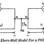
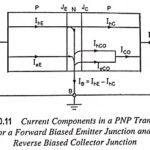
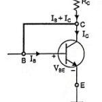
Transistor Lead Identification and Testing

Transistor Lead Identification and Testing: Transistor Lead Identification and Testing - After the transistor has been manufactured, as already discussed, leads of, typically, gold, aluminium, or nickel are then attached…

Continue Reading Transistor Lead Identification and Testing

Early Effect and Base Width Modulation

Early Effect and Base Width Modulation: In active region, the emitter-base (EB) junction is forward biased and collector-base (CB) junction is reverse biased, so the barrier width at EB junction…

Continue Reading Early Effect and Base Width Modulation

Transistor Circuit Configurations (CB, CE, CC)

Transistor Circuit Configurations (CB, CE, CC): As already mentioned, a Transistor Circuit Configurations is a three-terminal device (having three terminals namely emitter, base and collector) but we require four terminals—two…

Continue Reading Transistor Circuit Configurations (CB, CE, CC)

Ebers Moll Model for PNP Transistor

Ebers Moll Model for PNP Transistor: Device modelling aims at relating physical device parameters to device terminal characteristics. Device modelling is especially important for integrated circuits, since simple and accurate…

Continue Reading Ebers Moll Model for PNP Transistor

Explain Transistor Current Components

Explain Transistor Current Components: The various transistor current components which flow across the forward-biased emitter junction and reverse biased collector junction are indicated in Fig. 10.11. The current flowing into…

Continue Reading Explain Transistor Current Components