Metallization Process | Types of Metallization | Applications:
Metallization Process in which a thin layer of metal is formed which is used to make interconnections between the components on the chip as well as interconnections between the components and the outside world.
In general metallization applications are divided into three groups,
- Gate,
- Contact and
- Interconnects.
In VLSI, different new Metallization Process schemes for gate, interconnections, ohmic contacts are introduced. But the application of any new metallization scheme is tested in accordance with certain requirements as given below.
- The metal layer should be of low resistivity.
- The formation of layer should be easy.
- The layer should be easy for pattern generation to etched off.
- The layer should be stable in oxidizing ambients.
- The layer should have surface smoothness; mechanically stable with low stress and good adherence.
- The layer should not react with final metal.
- The metal should not contaminate devices, wafers.
- The device characteristics should be good enough.
Based on the types of applications there are three types of Metallization Process namely
1. Gate metallization:
The metallization which connects a base (in bipolar transistors) or gate (in MOSFETs) to the neighbouring two regions is called gate metallization.
2. Contact Metallization:
The metallization which is directly in contact with semiconductor is called contact metallization.
3. Interconnection Metallization:
The metallization which connects number of bipolar devices or MOSFETs is called interconnection metallization.
Metals and Alloys for Metallization:
In most of the IC’s, aluminium is the widely used metal for metallization because
- it is a good conductor
- it can form mechanical bonds with silicon
- it can form loW resistance, ohmic contacts with heavily doped n-type and p-type silicon.
But now a days alongwith aluminium, platinum silicide (Pt Si) has been used as a schottky barrier contact. It may be used as an ohmic contact simply for deep junctions. For high reliable connections to the outside, platinum / titanium / gold beam lead technology is prefered.
Actually no metal satisfies all the desired properties. Eventhough aluminium is most widely used metal, it has certain drawbacks such as :
- low melting point
- undesirable electromigration behaviour.
In MOS devices, polysilicon is generally used for gate metallization. With this metal in contact with gate oxides, devices characteristics and processes are unaltered. To have low resistance at gate and interconnection level, polysilicon is replaced by polysilicon /refractory silicides.
In the production of microprocessors and RAMs, refactor silicides with highest compatibility are used. The common examples are molybdenum (MoSi2), tantalum (TaSi2) and tungston (WSi2) which are all disilicides.
Because of junction spiking, high contact resistance, electromigration resistance, contact failure takes place. The contact problems can be overcome by using (i) Si-Alalloy, polysilicon layers gate and aluminium, (iii) selectively deposited tungston. Some times self aligned silicide such as platinum silicide (PtSi) is used in between silicon and silicide to ensure high metallurgical contact.
When aluminium is used as a top metal there is a possibility of interaction of silicide with aluminium in the 200 to 500° C temperature range. To overcome this, transition metal nitrides, carbides and borides are used as barrier between silicide and aluminium.
Lastly the most important characteristics of a Metallization Process is that it should be good adhesive. From that point of view, the metals, forming oxides, such as Al, Ta, Tl etc are most commonly used. The titanium is the most commonly used metal providing good adherence. The important property of titanium is that it forms a good bond with SiO2 at two temperatures and acts as a glue layer.
The following Table 1.5 gives the list of metals and alloys used for different metallization applications.
| Metallization | Metals / Alloys | |
| 1. | Gates, contacts and interconnections. | Polysilicon, silicides, nitrides, carbides, borides, refractory metals, aluminium and alloys of two or three of above. |
| 2. | Top level. | Aluminium. |
| 3. | Diffusion barrier. | Nitrides, carbides, silicides, borides. |
| 4.. | Selectiyely formed. | Tungston, aluminium and silicides. |
The important properties of the metallization are
- resistivity (μΩ-cm),
- melting point (°C), and
- linear thermal expansion coefficient (ppm/ ° C)
The resistivity ρ for the pure, thick and single crystalline film is lower ; while for impure and grain boundaries, it is higher. Due to chemical or metallurgical interactions, the resistivity of metallization either increases or decreases.
The second important property is the melting point. The solid state diffusion controls grain growth, annealing of defects as well as interactions in solid state. It is observed that the solid state is effective only at a temperature larger than one third of the melting point of the solid in which diffusion takes place.
The last property is the thermal expansion coefficient a. If there is a difference between the thermal expansion coefficients of the film and substrate, the stress conditions are observed on thin films. The stress will be greater, if the difference between the thermal expansions coefficients is more. The silicides show large stress conditions. This internal stress is balanced by a substrate producing opposite stress. Thus for proper formation of metal layer on substrate, the film stresses and factors affecting must be studied in detail.
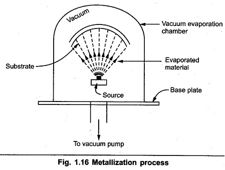
The Metallization Process takes place in a chamber which is called vacuum evaporation chamber. The chamber pressure is adjusted to the range of 10-6 to 10-7 Torr. The material to be evaporated is placed in a basket. Then using electron gun, high power density electron beam is focused at the surface of the material. Due to this, material starts heating up and vaporizing. These vapours hit substrate and condence there to form a thing film coating. After the metalization process is over, the thin film is patterned to form required interconnections. By using proper etching process, aluminium is removed form unwanted places.
In general, there are two important deposition processes.
1. Chemical vapour deposition:
This process has number of advantages over other process such as, (i) low temperature process, (ii) high throughput, and (iii) excellent step coverage.
Using chemical vapour deposition technique only Molybdenum and tungston is depositied. This process is carried at low pressure, hence also known as LPCVD. Using laser CVD, selective area deposition or direct writing throughout, both is possible.
2. Physical vapour deposition:
There are two types of physical vapour deposition processes namely evaporation and sputtering. In both the processes, first the condensed phase of the solid is converted into gaseous or vapour phase. Then the gaseous phase of the solid is transported to the substrate. And then lastly the gaseous source is condensed on the substrate followed by film growth.
The evaporation method is the simplest method of film deposition by the condensation of a vapour on a substrate. In this method, the temperature of the substrate is maintained lower than that of the vapour. When any metal is heated to sufficiently high temperature, it vapourizes. To heat a metal to high temperature different methods of heating are used such as resistance heating, inductive heating, electron bombardment and laser heating. For aluminium, which is the most common metal used for Metallization Process, any of the methods can be used.
In sputter deposition, unlike evaporation method, energetic ions are bombarded on the target material. Due to this process, some atoms of the target materials are released. These released atoms are then condensed on the substrate. The sputtering deposition process is applicable to any type of materials such as ‘ insulators, semiconductors, metals or alloys. As compared to evaporation process, the sputtering process is well controlled. This is carried at relatively high pressures like 1 Pa.
Metallization Applications:
- Gate and interconnection metallization controls the speed of the circuit by controlling the resistance of the interconnection lines. For high speed operation, such resistance should be as small as possible.
- The gate and interconnection metallization also controls flat band voltage VFB, which is essential to maintain a flat band condition in the
- The contact metallization gives electrically and mechanically stable ohmic contact having contact resistance negligibly small compared to the device
- The top level metal is thick as it carries current which provides connection to the outside world.
The metallization is used to, produce rectifying contacts and diffusion barriers between reacting metallic film