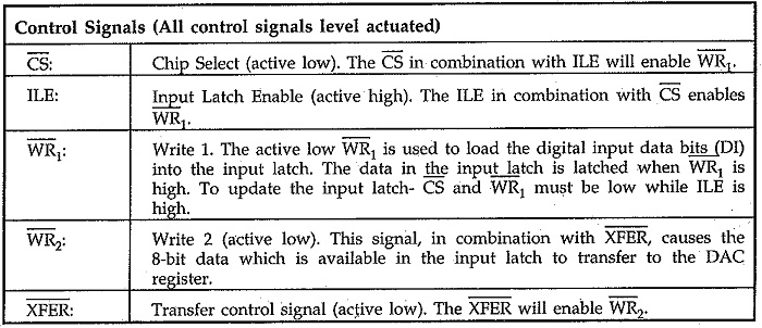
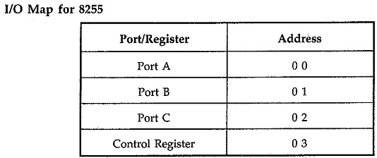
DAC0830 Digital to Analog Converter:
The DAC0830 Digital to Analog Converter is an advanced CMOS 8-bit DAC designed to interface directly with the 8080, 8048, 8085, Z80, and other popular microprocessors. A deposited silicon-chromium R-2R resistor ladder network divides. the reference current and provides the circuit with excellent temperature tracking characteristics (0.05% of Full Scale Range maximum linearity error over temperature). The circuit uses CMOS current switches and control logic to achieve low power consumption and low output leakage current errors. Special circuitry provides TTL logic input voltage level compatibility.
Double buffering feature allows this DAC to output a voltage corresponding to one digital word while holding the next digital word. This permits the simultaneous updating of any number of DACs.
The DAC0830 Digital to Analog Converter series (DAC0830/DAC0831/DAC0832) are the 8-bit members of a family of microprocessor-compatible DACs. For applications demanding higher resolution, the DAC1000 series (10-bits) and the DAC1208 and DAC1230 (12-bits) are available alternatives.
Features:
- Double-buffered, single-buffered or flow-through digital data inputs.
- Easy interchange and pin-compatible with 12-bit DAC1230 series.
- Direct interface to all popular microprocessors.
- Built-in facility for zero adjustment.
- Works with ± 10V reference voltage.
- Can be used in the voltage switching mode.
- Logic inputs which meet TTL voltage level specifications.
- Operates “STAND ALONE” (without up) if desired.
- Available in 20-pin small-outline or molded chip carrier package.
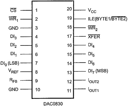
Pin Diagrams:
Fig. 14.111 shows the pin diagram of DAC0830 Digital to Analog Converter. The function of each pin is explained in Table 14.12.
Functional Block Diagram:
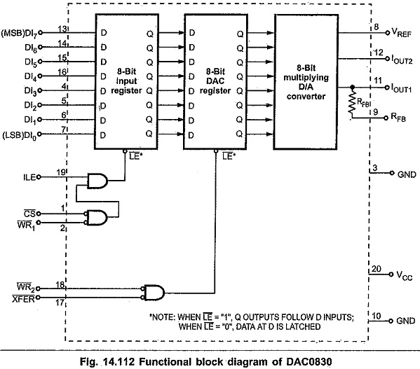
A most unique characteristic of this DAC is that the 8-bit digital input byte in double-buffered, as shown in the Fig. 14.112. This means that the data must transfer through two independently controlled 8-bit latching registers before being applied to the R-2R ladder network to change the analog output. The addition of a second register allows two useful control features. First, any DAC in a system can simultaneously hold the current DAC data in one register (DAC register) and the next data word in the second register (input register) to allow fast updating of the DAC output on demand. Second, and probably more important, double-buffering allows any number of DACs in a system to be updated to their new analog output levels simultaneously via a common strobe signal.
Double-Buffered Operation:
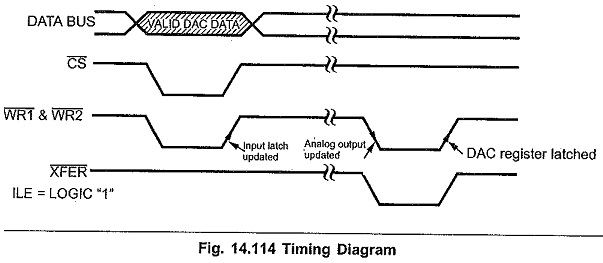
Updating the analog output of this DAC in a double-buffered manner is basically a two step or double write operation. In a microprocessor system two unique system addresses must be decoded, one for the input latch controlled by the CS pin and a second for the DAC latch which is controlled by the XFER line. If more than one DAC is being driven, Fig. 14.113, the CS line of each DAC would typically be decoded individually, but all of the converters could share a common XFER address to allow simultaneous updating of any number of DACs. The timing for this operation is shown, Fig. 14.114.
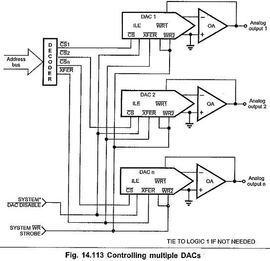
It is important to note that the analog outputs that will change after a simultaneous transfer are those from the DACs whose input register had been modified prior to the XFER command.
The ILE pin is an active high chip select which can be decoded from the address bus as a qualifier for the normal CS signal generated during a write operation. This can be used to provide a higher degree of decoding unique control signals for a particular DAC, and thereby create a more efficient addressing scheme.
Another useful application of the ILE pin of each DAC in a multiple DAC system is to tie these inputs together and use this as a control line that can effectively “freeze” the outputs of all the DACs at their present value. Pulling this line low latches the input register and prevents new data from being written to the DAC. This can be particularly useful in multiprocessing systems to allow a processor other than the one controlling the DACs to take over control of the data bus and control lines. If this second system were to use the same addresses as those decoded for DAC control (but for a different purpose) the ILE function would prevent the DACs from being erroneously altered.
Analog Output:
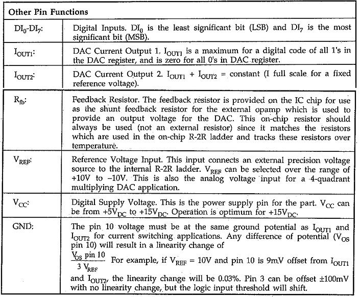
In the case of the DAC0830 Digital to Analog Converter, the output, IOUT1, is a current directly proportional to the product of the applied referenced voltage and the digital input word. For application versatility, a second output, Tarn, is provided as a current directly proportional to the complement of the digital input. Basically:
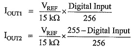
where the digital input is the decimal (base 10) equivalent of the applied 8-bit binary word (0 to 255), VREF is the voltage at pin 8 and 15 kΩ is the nominal value of the internal resistance, R, of the R-2R ladder network.
Typical Connection:
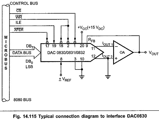
Fig. 14.115 shows the typical connection to interface DAC0830 Digital to Analog Converter to a microprocessor. As shown in the Fig. 14.115, microprocessor sends digital data to DAC through the data bus. The DAC0830 gives the converted output in current form and this output is converted into voltage form by external op-amp.
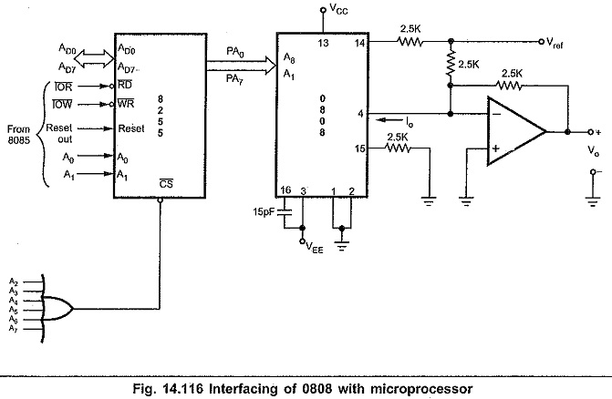
Interfacing 1408/0808 DAC with 8085:
Fig. 14.116 shows the interfacing of DAC 0808 with microprocessor 8085. Here, programmable peripheral interface, 8255 is used as parallel port to send the digital data to DAC.
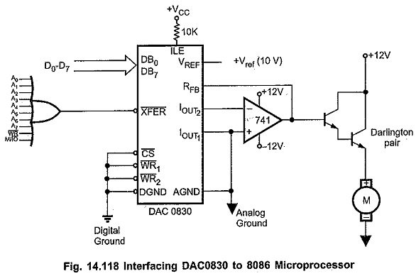
Interfacing DAC 0830 with 8086:
The DAC0830 Digital to Analog Converter is connected to 8086 microprocessor, as shown in the Fig. 14.118. Here, I/O port address is decoded using_ OR gate. The digital data is loaded into DAC0830 when A0-A7 lines, WR and IO/M signals are low. This gives us the address for DAC0830 as 00H and the data can be loaded in the DAC0830 by OUT 00H,AL instruction, where AL register contains the digital data to be sent to DAC0830. The IC 741, the operational amplifier is used to convert current output of DAC0830 to voltage output. The voltage output of the operational amplifier is used to drive the DC motor after increasing the driving capacity. The driving capacity is increased by using the darlington transistor.
Interfacing DAC0830 with 8086 Using 8255: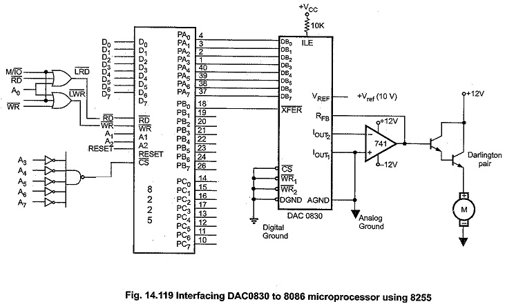
Fig. 14.119 (see on previous page) shows the interfacing of DAC0830 to 8086 Microprocessor using 8255. Here, port A of 8255 is used to send data to the DAC0830 and the XFER signal is generated by programming PB0 pin of 8255. The 8255 is interfaced to 8086 system in I/O mapped I/O with address : PA = 00H, PB = 02H, PC = 04H, PC= 06H.