Digital to Analog Converter Circuit Diagram:
The basic Digital to Analog Converter Circuit Diagram using Op Amp is shown in Fig. 17.18(a). The input signal is applied to the inverting terminal of the opamp.
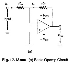
In Digital to Analog Converter Circuit Diagram the input impedance is almost infinity, and almost no current can enter the input terminals. The input voltage is fixed to almost zero at its input terminals; the upper terminal is at nearly the same potential as the ground terminal. Therefore, the upper terminal is called a virtual ground.
The difference between virtual ground and normal ground is zero, while sinking any amount of current. Virtual ground is for voltage, not for current. Therefore, virtual ground point is at 0 V, i.e. it sinks current.
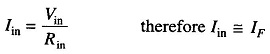
Because no current can enter the virtual ground (because of ∞ impedance) all the current has to go through RF with respect to the virtual ground. Vout is measured with respect to normal ground.