Semiconductor Articles:
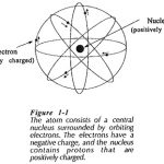
Introduction to Semiconductor Materials and Devices: An electronic device controls the movement of electrons. The study of electronic devices requires a basic understanding of the relationship between electrons and the other components of an atom. The movement of electrons within a … (Read More)
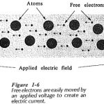
Conduction in Solids: Conduction in Solids or any given material occurs when an applied voltage causes electrons within the material to move in a desired direction. This may be due to one or both of two processes; Electron Motion and Hole … (Read More)
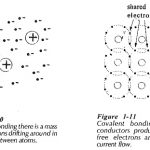
Conductor Semiconductor and Insulator: Bonding Forces Between Atoms: Whether a material is a Conductor Semiconductor and Insulator depends largely upon what happens to the outer-shell electrons when the atoms bond themselves together to form a solid. In the case of copper, … (Read More)
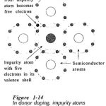
P Type and N Type Semiconductor: Doping : Pure semiconductor material is known as intrinsic material. Before intrinsic material can be used for device manufacture, impurity atoms must be added to improve its conductivity. The process of adding the atoms is … (Read More)
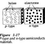
PN Junction Semiconductor: Two blocks of PN Junction Semiconductor material are represented in Fig. 1-17; one block is p-type material, and the other is n-type. The small circles in the p-type material represent holes, which are the majority charge carriers in … (Read More)
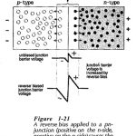
Reverse Bias PN Junction: When an external bias voltage is applied to a pn-junction, positive to the n-side and negative to the pride, electrons from the n-side are attracted to the positive terminal, and holes from the p-side are attracted to … (Read More)
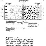
PN Junction Forward Bias: Consider the effect of an external bias voltage applied with the polarity of PN Junction Forward Bias shown in Fig. 1-23; positive on the p-side, negative on the n-side. The holes on the p-side, being positively charged … (Read More)