JFET Biasing Circuits
JFET Biasing Circuits: Use of Plus/Minus Supplies - When plus/minus supply voltages are to be used with a JFET Biasing Circuits, the gate terminal is usually grounded via RG, as…
Continue Reading
JFET Biasing Circuits
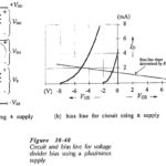
JFET Biasing Circuits: Use of Plus/Minus Supplies - When plus/minus supply voltages are to be used with a JFET Biasing Circuits, the gate terminal is usually grounded via RG, as…
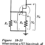
JFET Bias Circuit Troubleshooting: Voltage Measurement - JFET Bias Circuit Troubleshooting are similar to those for BJT bias circuits. The major difference is that there is only one junction in…
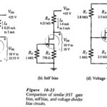
Basic JFET Biasing Circuits Comparison: The Basic JFET Biasing Circuits Comparison (gate bias, self-bias, and voltage divider bias) are similar in performance to the three basic BLIP bias circuits, (base…
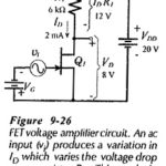
FET Amplification: Consider the n-channel FET Amplification circuit in Fig. 9-26. Note that drain-source terminals are provided with a dc supply (VDD), connected via the drain resistor (R1). The gate-source…
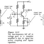
High Frequency Analysis of BJT: Coupling and Bypass Capacitor Effects - Consider the typical High Frequency Analysis of BJT illustrated in Fig. 8-5. As discussed, the amplifier voltage gain is…
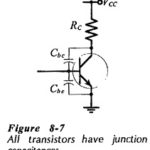
BJT Cutoff Frequency and Capacitance: Device Cutoff Frequency - All transistors have junction capacitances. The junction capacitances and the transit time of charge carriers through the semiconductor material limit the…
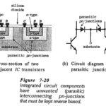
Integrated Circuit Components: The Integrated Circuit Components are namely, Transistors and Diodes: The epitaxial planar diffusion process described already is normally employed for the manufacture of IC transistors and diodes. Collector,…
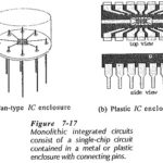
Integrated Circuits Fabrication Process: IC Types - An Integrated Circuits Fabrication Process consists of several interconnected transistors, resistors, etc., all contained in one small package with external connecting terminals. The…