Field Effect Transistors Articles:
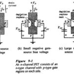
Junction Field Effect Transistor Theory: n-Channel JFET – The operating principle of an n-channel Junction Field Effect Transistor Theory (JFET) is illustrated by the block representation in Fig. 9-1(a). A piece of n-type semiconductor material, referred to as the channel, is … (Read More)
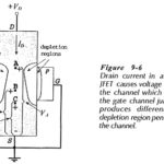
JFET Characteristics: An n-channel JFET Characteristics block representation is shown in Fig. 9-6. With a drain-source voltage applied as illustrated, ID flows in the direction shown producing voltage drops along the channel. Consider the voltage drops from the source terminal (S) … (Read More)
FET Datasheet Specifications: Maximum Ratings – A portion of a FET Datasheet Specifications is reproduced in Fig. 9-17. As with other device data sheets, a device type number and brief description is usually given at the start. Maximum ratings follow, and then the … (Read More)
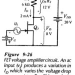
FET Amplification: Consider the n-channel FET Amplification circuit in Fig. 9-26. Note that drain-source terminals are provided with a dc supply (VDD), connected via the drain resistor (R1). The gate-source junctions are reverse-biased by the gate voltage (VG). An ac signal … (Read More)
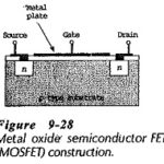
MOSFET Construction and Characteristics: Figure 9-28 shows the MOSFET Construction and Characteristics of a metal oxide semiconductor FET (MOSFET), also known as an insulated gate FET. Starting with a high-resistive p-type substrate, two blocks of heavily-doped n-type material are diffused into … (Read More)