BJT Biasing

Biasing Transistor Switching Circuits

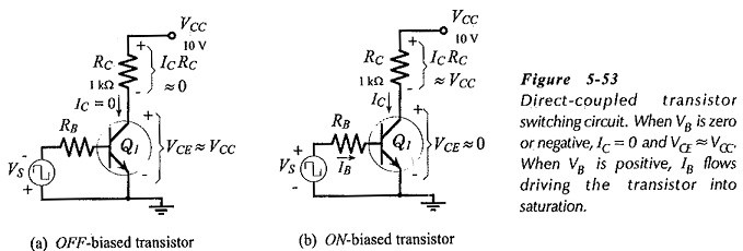
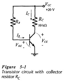
Biasing Transistor Switching Circuits: Direct-Coupled Switching Circuit – When a transistor is used as a Biasing Transistor Switching Circuits, it is either biased off to IC = 0, or biased on to its maximum collector current level. Figure 5-53 illustrates the two conditions. Note that the circuit in Fig, 5-53 is termed a direct-coupled switching […]

Biasing Transistor Switching Circuits Read More »

Bias Circuit Thermal Stability

Bias Circuit Thermal Stability: VBE and ICBO Variations – Many transistor circuits are required to operate over a wide temperature range. So, another aspect of bias circuit stability is Bias Circuit Thermal Stability, or how stable IC and VCE remain when the circuit temperature changes. Measures to deal with the effects of hFE variations have already been

Bias Circuit Thermal Stability Read More »

Bias Circuit Design

Bias Circuit Design: Bias Circuit Design can be amazingly simple. Usually, it is just a matter of determining the required voltage across each resistor and the appropriate current levels. Then, the resistor values are calculated by application of Ohm’s law. Designs usually begin with specification of the supply voltage and the required levels of IC

Bias Circuit Design Read More »

BJT Bias Circuit Troubleshooting

BJT Bias Circuit Troubleshooting: Voltage Measurement – When a BJT Bias Circuit Troubleshooting is constructed in a laboratory situation, the supply voltage (VCC) and the voltage levels at the transistor terminals (VC, VB and VE) should be measured with to the ground or negative supply terminal, as illustrated in Fig. 5-32. When the measured voltages are

BJT Bias Circuit Troubleshooting Read More »

Comparison of Different Biasing Circuits

Comparison of Different Biasing Circuits: The Comparison of Different Biasing Circuits of the three basic bias circuits, it must be recalled that transistor manufacturers specify maximum and minimum hFE values for each transistor type number at various levels of collector current. Normally, the current gain of each individual transistor is not known, so that (as already

Comparison of Different Biasing Circuits Read More »

Voltage Divider Bias Circuit

Voltage Divider Bias Circuit: Circuit Operation – Voltage Divider Bias Circuit, also known as emitter current bias, is the most stable of the three basic transistor bias circuits. A voltage divider bias circuit is shown in Fig. 5-22(a), and the current and voltage conditions throughout the circuit are illustrated in Fig. 5-22(b). It is seen

Voltage Divider Bias Circuit Read More »

Collector to Base Bias Circuit

Collector to Base Bias Circuit: The Collector to Base Bias Circuit shown in Fig. 5-17(a) has the base resistor (RB) connected between the transistor collector and base terminals. As will be demonstrated, this circuit has significantly improved bias stability for hFE changes compared to base bias. Refer to Fig. 5-17(b) and note that the voltage

Collector to Base Bias Circuit Read More »

Base Bias in BJT

Base Bias in BJT: Circuit Operation and Analysis – The transistor bias arrangement shown in Fig. 5-12 is known as Base Bias in BJT and also as fixed current bias. The base current is a constant quantity determined by supply voltage VCC and base resistor RB. Because VCC and RB are constant quantities. IB remains fixed

Base Bias in BJT Read More »

Scroll to Top