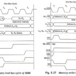
Timing Diagram of the 8088 Microprocessor
Timing Diagram of the 8088 Microprocessor: Each bus cycle of the 8088 processor consists of four T states: T1, T2, T3 and T4. During the first clock cycle T1, ALE signal is high…
Continue Reading
Timing Diagram of the 8088 Microprocessor