Pentium Pro, Pentium II and Pentium III Processors:
Pentium Pro The Pentium Pro is a sixth-generation x86 microprocessor and it was introduced by Intel in 1995. This processor was developed based on the P6 micro-architecture. The Pentium and Pentium MMX processors have 3.1 and 4.5 million transistors respectively, but the Pentium Pro consists of 5.5 million transistors. The Pentium Pro is capable of both dual-processor and quad-processor configurations. The common features of Pentium Pro are given below:
- The Pentium Pro has a 12-stage decoupled super pipeline architecture which uses an instruction pool.
- It has extra decoded stages to dynamically translate IA-32 instructions into a sequence of buffered micro-operations.
- It has speculative execution through register renaming with 40 registers.
- It has dynamic program execution.
- Pentium Pro has a 36-bit address bus.
- It has an 8 KByte instruction cache. It has separate L1 code and data caches with write back strategy.
- It has data forwarding and dynamic branch prediction.
- The Pentium Pro has two integer units and one floating-point unit. One of the integer units shares the same ports as the FPU.
- It has an integrated L2 cache into processor core connected over a dedicated bus running at the CPU clock pulse (half or full).
- In the Pentium Pro processor, x86 instructions are decoded into 118-bit micro-operations (micro-ops).
- The Pentium Pro processor clock speeds are 150, 166, 180 or 200 MHz with a 60 or 66 MHz external bus clock.
- This processor is very popular in multiprocessing configuration.
- P6 architecture operates with 32-bit OS such as Windows NT 3.5, Unix and OS/2.
- It is packaged in ceramic multi-chip modules (MCM). The MCM has 387 pins which is approximately half of pin grid array (PGA) package. The MCM package was designed for Socket 8.
- Pentium Pro processor core operates at 3.1 V to 3.3 V.
- Pentium Pro is fabricated in a 0.6 μm BiCMOS process for 133 MHz operating frequency, in a 0.5 μm BiCMOS process for 150 MHz, and in a 0.35 μm BiCMOS process for 166, 180, and 200 MHz.
Pentium II After the Pentium Pro processor, Pentium II was developed by Intel in 1997. Pentium II is manufactured based on P6 micro-architecture and it is a sixth-generation x86 compatible microprocessors. This processor core contains 7.5 million transistors and it is an improved version of the first P6-generation core of the Pentium Pro. All features of the Pentium Pro have been incorporated with Pentium II. This processor has a larger cache. As this processor can operate at 2.8 V, the power consumption is reduced significantly. Pentium II can support MMX instructions for enhanced floating-point operation. The features of Pentium II processor are given below:
- The L2 cache size is increased to 512 KB from the 256 KB on the Pentium Pro. The L2 cache operates at half of the processor’s clock frequency, whereas the L2 cache of Pentium Pro operates at the same frequency as the processor.
- The Pentium II has a 32 KB L1 cache which is double Of the Pentium Pro. This processor has separate 16 KB L1 data and 16 KB L1 instruction caches.
- The 16-bit code execution performance is available on the Pentium II processor.
- The Pentium II is a consumer-oriented version of the Pentium Pro. It is cheaper to manufacture because of the separate slower L2 cache memory.
- The improved 16-bit performance and MMX support make it suitable for Windows operating systems and multimedia applications.
- The Pentium II is packaged in a slot-based module rather than a CPU socket.
- The Pentium II processor clock speeds are 233, 266, 300, 350, 400 or 450 MHz with a 66 MHz front side bus.
- Pentium II Klamath (80522) processor core operates at 2.8 V, and Pentium II Deschutes (80523) processor core operates at 2.0 V.
- Pentium II Klamath is fabricated in a 0.35 μm CMOS process and Pentium II Deschutes is fabricated in a 0.25 μm CMOS process.
Pentium III After the Pentium II, the next version of the Pentium processor is Pentium III. This processor was developed by Intel in 1999. Pentium III is a sixth-generation x86-compatible microprocessor and it was manufactured based on P6 micro-architecture. This processor core contains 9.5 to 28 million transistors. All features of the Pentium II have been added with Pentium III. This processor is used for high-performance desktop computers and servers which can operate Windows NT, Unix and Windows 98 operating systems. This processor is suitable for audio and video processing, image processing, and Internet and multimedia applications. The new features of the Pentium III processor are given below:
- Pentium III can operate in multiple branch prediction algorithms.
- 70 new instructions are added to the Pentium III for multimedia and advanced image processing This processor has SSE (streaming SIMD) extensions.
- It can support dynamic execution technology.
- Pentium III has eight 64-bit Intel MMX registers and 57 MMX instructions for multimedia applications.
- It has an on-die 512 Kbyte L2 cache.
- This processor is available at operating frequencies of 450 MHz to 1.4 GHz with 100 MHz to 133 MHz front side bus.
- Pentium III can operate at 2.0 V to 1.45 V.
- Pentium III Katmai is fabricated in a 0.25 μm CMOS process, Pentium III Coppermine is fabricated in a 0.15 μm CMOS process and Pentium III Tualatin is fabricated in a 0.13 μm CMOS process.
In this section, the internal architecture, instruction pool, 36-bit address bus and paging mechanism of P6 family processors are discussed elaborately.
Architecture of P6 Family Processors The block diagram representation of internal architecture P6 family processors is depicted in Fig. 12.54. It is clear from Fig. 12.54 that the P6 family processor has a Bus Interface Unit (BIU), L1 data cache, L1 code cache, instruction fetch unit, instruction decoder, Branch Target Buffer (BTB), Register Alias Table (RAT), Reservation Station (RS), retire unit and on-chip Advanced Programmable Interrupt Controller (APIC).
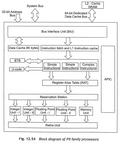
Bus Interface Unit (BIU) The bus interface unit is used to interface between system bus, 64-bit dedicated cache bus and L1 code and L1 data caches.
L1 Data Cache The L1 data cache is organized as two-way set-associative cache organization. Pentium Pro processor has 8 Kbyte data cache but Pentium II and Pentium III processors have 16 Kbyte data cache with two access ports. The write access (write port) and a read access (read port) can be occurred simultaneously. The data cache can support all 4 MESI protocol states.
L1 Code Cache The L1 cache is also organized in two-way set-associative cache organization. The pentium Pro processor an has 8 Kbyte code cache whereas Pentium II and Pentium III processors have 16 Kbyte code cache. The code cache supports only two states of 4 MESI protocol states, i.e., S and I states.
Instruction Fetch and Decoder In the instruction fetch stage, instructions are fetched from the instruction cache. After that instructions are decoded. There are 3 decode units in the instruction decoder and they are operating in parallel. Two decode units are used to decode simple instructions that microcodes are not required for simple instructions and the third decoder is used to decode CISC or complex instructions that require a microcode. Usually, instructions are decoded into sequences of μ-ops.
Branch Target Buffer (BTB) The branch target buffer is used to store 512 branch targets along with information to predict branches correctly. The BTB is also required for speculative execution due to the length of the pipeline.
Internal Registers The P6 family, such as Pentium Pro, Pentium II and Pentium III processors have 40 internal registers. These processors use these registers in place of the x86 registers. Actually, the Register Alias Table (RAT) remaps the x86 registers from the instruction to the 40 internal registers by using the register-renaming technique.
Reservation Station and Execution Unit In P6 processors, there are five execution units which consist of two integer units INT-I and INT-II, two floating-point units FPU-I and FPU-II, and a Memory Unit (MU). The reservation station is used to sends instructions to the above five execution units. All five execution units work independently. In best conditions, execution of five instructions can be completed in one clock pulse.
Retire Unit and APIC The retire unit resolves data dependencies. This unit can verify branches and writes to the x86 architectural registers. The on-chip advanced programmable interrupt controller supports multiprocessing with up to 4 processors.
Instruction Pool of P6 Family Processors The P6 family Pentium processors have 3 pipelines and each pipeline has 12 stages. The 12 stages generate data-dependency problems and pipeline stalls. The P6 processors have decoupled pipelines and the simple execution stage is replaced by the two decoupled phases, namely, dispatch/execute unit and retire unit. In the decoupling method, the instructions in the pipelines are executed independently. Therefore, the instructions can be executed out-of-order in the Instruction Pool. Figure 12.55 shows the instruction pool of P6 family processors.
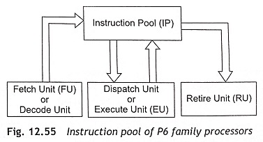
Instruction Fetch/Decode Unit The instruction fetch (IF)/decode unit reads the sequence of instructions from the instruction cache and decode them. The pre-fetching is performed in a speculative manner. Actually, IF/Decode unit reads 32 bytes or one cache line per clock from the L1 cache. This unit marks the start and end of the instructions and carries out branch prediction. After that, the IF unit transfers 16 byte to the decode unit
Decoder Unit The decoder unit has three parallel decoders. Two decoders are used for simple instructions and one decoder is used for complex instructions. The decoders accept the stream of fetched instructions and decode them. Actually, the decoders translate x 86 instructions into micro-operations (1-ops). Each micro-operation consists of two logical sources and a logical destination. Simple instructions are translated into single μ-ops and complex instructions are converted into a string of up to 4 μ-ops. The decoder generates up to 6 μ-ops in each clock pulse. The decoder maps references to available x86 and P6 registers. Only micro-operations (μ-ops) are executed in the execution units. Therefore, μ-ops are stored in the Register Alias Table (RAT). The RAT translates the logical register references to the physical register, which are available in P6 processors. Translation is performed in order in the IF/Decode unit. The IF/Decode unit transfers p-ops to the instruction pool. The pool of instructions is stored as an array of content addressable memory, which is known as reorder buffer. After that dynamic execution starts.
Dynamic execution of instructions states that instructions are stored in any order, but execution will be completed in the programmed order. Instruction pool is commonly available to the following three units: (i) start-in order. (ii) middle-out of order, and (iii) end-in order.
Dispatch/Execution Unit The dispatch/execution unit does the scheduling of instructions and controls dynamic instruction. This unit distributes μ-ops to the five execution units and a maximum of 5 μ-ops can be issued per clock cycle.
Instruction Pool The instruction pool has normally 20 to 30 μ-ops awaiting execution. Each micro-operation assigned information is used to indicate preparation, execution and final result states. A μ-ops is ready for execution whenever it is ready with operands. The instruction pool starts execution by transferring the ready μ-ops to the dispatch/execute unit. When an instruction is not ready, the instruction pool looks for another instruction which is ready. Results of 20-30 foresightedly executed instructions are stored in the registers of P6 processors. μ-ops can also be speculatively executed after a branch and results are returned to the instruction pool.
Retire Unit The retirement of instructions does not occur until execution of the instruction has been completed and their results are written back to the x86 registers. The retire unit reads instruction pool for completed instructions and removes the micro-operations, which have been already executed from the instruction pool. Maximum 3 μ-ops can be retired and removed from the instruction pool per clock.
36-Bit Address Bus and Paging Mechanism of P6 Family Processors
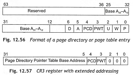
To support the 32-bit physical addresses, the paging data structure has the following changes:
- The page-table entries have been increased to 64 bits to incorporate 36-bit physical address as depicted in Fig. 12.56. There are 512 entries for page directory and page table. Each page size is 4 Kbytes.
- A new table, namely, the page-di-rectory pointer table has been added to the linear address translation. The page directory pointer table has 4 entries and each entry contains 64 bits. This lies above the page directory in the hierarchy.
- The 20-bit page directory base addresses in the CR3 register is replaced by a 27-bit page directory pointer table base address A31-A5 as shown in Fig. 12.57. The page-directory-pointer table base address field provides the 27 most significant bits of the physical address of the first byte of the page-directory-pointer table. The table must be located on a 32-byte boundary.
- The linear address translation has been changed to allow mapping 32-bit linear address into larger physical address space.
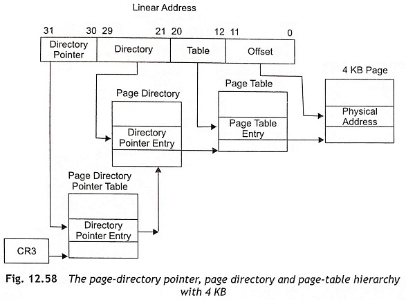
Figure 12.58 shows the page-directory pointer, page directory and page table during mapping linear address up to 4 Kbyte pages. A31-A30 of linear address are used for directory pointer to locate directory pointer entry in page directory pointer table. A29-A21 of linear address are used for directory to indicate directory entry of page directory. The page table entry is located by A20-A12 of the linear address and physical address is specified with the help of offset address A11-A0 with respect to page table entry. This paging technique can be used to address up to 220 pages and linear address space of 4 GB or 232 bytes. The 220 pages are computed from the following expression:
4 PDPTE x 512 PDE x 512 PTE = 220 pages
where,
- PDPTE = Page directory pointer table entry
- PDE = Page directory entry
- PTE = Page table entry
Figure 12.59 shows that the page-directory pointer and page directories can amplify linear address to 4 MByte or 2 MByte pages. It is clear from Fig. 12.59 that A31-A30 of linear address are used to locate directory pointer entry in the page-directory pointer table. Directory entry is addressed by A29-A21 of linear address and the physical address is located by the offset address of linear address A20-A0 with respect to directory entry. This paging method can be used to map up to 2048 pages and 4 GB linear address space. The computation of 2048 pages is given below:
4 PDPTE x 512 PDE = 2048 pages
where,
- PDPTE = Page directory pointer table entry and
- PDE = Page directory entry