What is Risc Processors?:
What is Risc Processors? – In the previous sections, CISC processors were discussed elaborately. CISC is pronounced sisk, and it stands for Complex Instruction Set Computer. Most desktop computers and laptops use CPUs based on this architecture. Usually, CISC ICs have a large amount of different and complex instructions. The philosophy behind CISC processors is that hardware is always faster than software. Therefore, one should make a powerful instruction set, which provides programmers with assembly instructions to do a lot of tasks with very short programs. The example of CSIC microprocessors are Intel 80486, Pentium, Pentium Pro, Pentium II, Celeron and Pentium III, etc. The common features of CISC processors are as follows:
Features of CISC Processors
- A CISC processor supports extensive complex instructions.
- It has complex and efficient machine instructions.
- It supports micro-encoding of the machine instructions.
- It has extensive addressing capabilities of memory operations.
- The CISC processor has less number of very useful CPU registers.
- The CISC processors can operate at relatively slow speed.
With incorporating the more and more complex instructions in a CISC, more and more sophisticated processors were developed, manufactured and used as CPUs of personal computers (PCs) for marketing. As a result, the processor die size was increased to accommodate the large numbers of microcode of the complex instructions. Due to large die size, CISC consumed more silicon and the chip size was increased. Consequently, the power consumption also increased, more heat sink was required for better cooling arrangement and cost of the system became high.
When a processor supports a set of simple instructions, it does not require complex decoding and the design process of the processor becomes very simple. Accordingly, costs of the system as well as power consumption are reduced significantly. The execution of the simple instructions is also very fast. In the mid-1970s, John Cocke at IBM research demonstrated that on microcoded implementations of CISC architectures, complex operations using complex instructions tended to be slower than a sequence of simpler operations doing the same thing. Processor designers also realized that in many cases, most of the complex instructions of a CISC processor’s instruction set are not actually used. In a typical CISC processor program, about 20% of the instruction set will perform about 80% operations of the program. Sometimes the execution of simple instructions is quicker than single complex machine instruction. Actually, the complex instructions will take a long time to decode, but simple instructions take less time to decode and execute faster. Therefore, simple instructions are most commonly used in programs and complex instructions are very rarely used.
Subsequently, RISC chips evolved around the mid-1980s as a reaction at CISC chips. RISC is pronounced risk, and it stands for Reduced Instruction Set Computer. The design philosophy behind RISC is that almost no one uses complex assembly-language instructions as used by CISC, and programmers mostly use compilers which never use complex instructions. RISC utilizes a set of fewer, simpler and faster instructions, rather than a more specialized set of instructions. However, more instructions are needed to accomplish a task in RISC. Generally, each instruction is executed within a single clock after it is fetched and decoded. To achieve this, RISC reduces decode and execute logic replacing microcode by hardwired logic gates and uses instruction pipelining techniques extensively. In a CISC, a lot of disc space is consumed by microcodes. As microcode is replaced by hardwired logic in RISC, the size of RISC processors becomes smaller than CISC and it consume less power.
The first attempt was taken to make a chip-based RISC CPU at IBM in 1975. After that, UC Berkeley and Stanford started work to design and develop RISC processors. After a long research, the IBM 801 was eventually developed in a single-chip form in 1981. After that Stanford MIPS (Microprocessor without interlocking Pipeline Stages), Berkeley RISC-I and RISC-II processors were developed. The examples of other microprocessors are DECs Alpha, power PC 601, 602, 603 and Ultra SPARC, etc. The common features of RISC processors are given below:
Features of RISC Processors
- Simple Instruction Set In a RISC processor, the instruction set consists of simple and basic The complex instructions can be composed using simple and basic instructions.
- Reduction of Instruction Set Less numbers of instructions are used to simplify instruction decoding.
- Elimination of Microcoding In RISC, microcode is replaced by hardwired logic gates. Hence all execution units are hardwired.
- Same Length Instruction Each instruction is of the same length.
- Single Machine–Cycle Instructions The execution of instructions complete in one machine cycle, which allows the processor to handle several instructions at the same time.
- Pipelining Usually, massive pipelining is used in a RISC processor. Due to pipelined instruction decoding and executing, more operations are performed in parallel. Therefore, the speed of RISC processors is increased.
- Very Few Addressing Modes RISC processors have very few addressing modes and it supports few formats.
- Load and Store Architecture In RISC processors, only the load and store instructions are used to access memory. Other instructions of the processor work with the internal registers of the processor.
- Large Number of Registers The RISC processors have a larger number of registers to reduce the interactions between the processor and memory.
The performance of a computer is computered by the following equation:
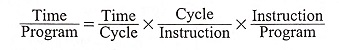
To get better performance, the CISC processors are designed to minimize the number of instructions per program sacrificing the number of cycles per instruction, but RISC processors are designed reducing the cycles per instruction at the cost of instructions per program.
Architecture of RISC PROCESSOR: Power PC 601
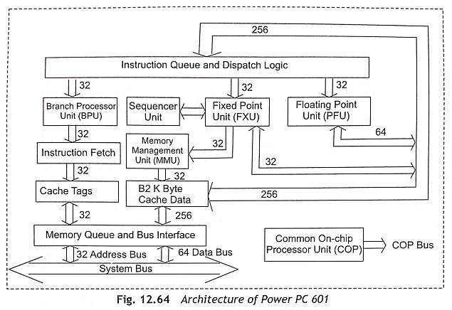
The IBM POWER (Performance Optimized with Enhance RISC) architecture is used as the base of Power PC architecture and RISC single-chip vector processor is the base of the 601 microprocessor. The Power PC 601 microprocessor is the first implementation of Power PC architecture and it was developed jointly by IBM and Motorola in 1993. The Power PC 601 is a 32-bit Power PC architecture processor. This processor has three instruction units, namely, Branch Processor Unit (BPU), Fixed-Point Unit (FXU), and Floating-Point Unit (FPU). These three execution units are used to support superscalar dispatch of instructions. The simplified block diagram of a Power PC 601 is shown in Fig. 12.64. The branch processor unit is a subpart of the main instruction unit and is used for fetching and perfecting instructions. A maximum of 8 instructions can be stored in the instruction fetch queue. The instruction unit can fetch instructions in the branch processor unit, fixed-point unit and, floating-point unit simultaneously and execute instructions in parallel on each unit.
The RISC processor pipeline operates in such a way that some operations may be carried out in parallel, although the stages in the pipeline are different. Though different processors have different number of steps to execute instructions, there are five steps that will be required when a processor executes an instruction. Figure 12.65 shows the pipeline structure of Power PC 601.
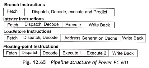
Step 1 Instruction fetch phase: Read the instruction from the memory or the prefetch queue.
Step 2 Decode phase: Read register and decode the instruction.
Step 3 Operand fetch phase: Fetch the operand whenever required for the instruction.
Step 4 Execute phase: Execute the instruction.
Step 5 Write-back phase: Write the result into the register.
The Power PC 601 has a 32 Kbyte unified L1 cache. The instruction queue and dispatch logic unit buffer instructions from 32 Kbyte unified cache and dispatch up to three instructions on each cycle: one each to the BPU, the FXU and the FPU. The fixed point unit communicates with the sequencer unit to control most frequently used instructions. The FXU interfaces with Memory Management Unit (MMU) for cache accesses.
The 32 Kbyte unified cache provides a 256-bit interface with instruction queue and memory queue, a 64-bit interface to the FPU and a 32-bit interface to the FXU. The Power PC 601 has a 32-bit address bus and a 64-bit data bus. This processor supports a Common On-chip Processor (COP) unit through a COP bus and an asynchronous serial port for debugging and test features.
MIPS
MIPS stands for ‘Microprocessor without Interlocked Pipeline Stages’. MIPS is a RISC architecture processor. The MIPS processor has 32 registers and each register is 32 bits wide. The instruction set of a MIPS processor consists 111 instructions such as 15 load instructions, 10 store instructions, 21 arithmetic instructions, 8 logic instructions, 12 comparison instructions, 8 bit-manipulation instructions, 8 move instructions, 25 branch/jump instructions and 4 miscellaneous instructions. The addressing modes as well as instruction set of RISC microprocessors are simpler and much less in numbers compared to the CISC microprocessors. All arithmetic and logical instructions operate in register mode of addressing and the operands are stored in the set of 32-bit registers. The load and store instructions are used as data-transfer instructions to store data in the register from memory and vice versa. The base displacement addressing mode is also used for data-transfer instructions. In this case, the effective address is generated by addition of the content of a base register and a displacement which already exists in the instruction.
Sun Ultra Sparc
The SPARC (Scalable Processor Architecture) is a unique RISC instruction set architecture. It was developed by Sun Microsystems and introduced in mid-1987. This processor consists of an integer unit, a floating-point unit, and an optional co-processor. Usually, the SPARC processor contains about 160 general-purpose registers but only 32 of them are immediately visible to software at any point of time. Among the 32 registers, eight registers are a set of global registers and the other 24 registers are local registers and are used as the stack of registers. These 24 registers form a register window. During function call and return, this window is moved up and down the register stack. Each window consists of 8 local registers and shares 8 registers with each of the adjacent windows. Generally, the shared registers are used for passing function parameters and returning values, but the local registers are used for storing local values across function calls. The different versions of Sun Ultra SPARC microprocessors are Ultra SPARC T1, Ultra SPARC T2, SPARC V8, SPARC V9, SPARC64 VI , SPARC64 VII, and SPARC T3, etc. The common features of SPARC architecture are given below:
- The SPARC processor has a 14-stage nonstalling pipeline.
- It has six execution units which consist of two integer units, two floating-point units, one LOAD/STORE unit and one address generation unit.
- This processor has a large number of buffers.
- As there is only one LOAD/STORE unit, it dispatches one instruction at a time.
- The ULTRA SPARC 3 processor has a 32 KB L1 code cache, a 64 KB L1 data cache, a 1 MB on chip L2 cache, a 2 KB prefetch cache and a 2 KB write cache.
- The SPARC system operates at low speed compared to other processors.
- ULTRA SPARC supports a pipelined floating-point processor:
This processor supports multimedia instructions just like Pentium MMX. Hence, this can be used for multimedia and image-processing applications.