Introduction to Semiconductor Materials and Devices:
An electronic device controls the movement of electrons. The study of electronic devices requires a basic understanding of the relationship between electrons and the other components of an atom. The movement of electrons within a solid, and the bonding forces between atoms can then be investigated. This leads to a knowledge of the differences between conductors, insulators, and semiconductors, and to an understanding of p-type and n-type in the introduction to semiconductor material.
Junctions of p-type and n-type material (pn-junctions) are basic to all but a very few semiconductor devices. Forces act upon electrons that are adjacent to a pn-junction, and these forces are altered by the presence of an external bias voltage.
Atomic Theory of Semiconductors:
The atom can be thought of as consisting of a central nucleus surrounded by orbiting electrons (see Fig. 1-1). Thus, it may be compared to a planet with orbiting satellites. Just as satellites are held in orbit by the attractive force of gravity due to the mass of the planet, so each electron is held in orbit by an electrostatic force of attraction between it and the nucleus.
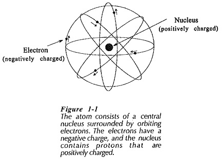
Each electron has a negative electrical charge of 1.602 x 10⁻¹⁹ coulombs (C), and some particles within the nucleus (protons) have a positive charge of the same magnitude. Since opposite charges attract, a force of attraction exists between the oppositely charged electron and nucleus. Compared to the mass of the nucleus, electrons are relatively tiny particles of almost negligible mass. In fact, they can be considered to be little particles of negative electricity having no mass at all.
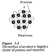
The nucleus of an atom (Fig. 1-2) is largely a cluster of two types of particles, protons and neutrons. Protons have a positive electrical charge, equal in magnitude (but opposite in polarity) to the negative charge on an electron. A neutron has no charge at all. Protons and neutrons each have masses about 1800 times the mass of an electron. For a given atom, the number of protons in the nucleus normally equals the number of orbiting electrons.
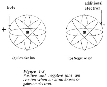
Since the protons and orbital electrons are equal in number and equal and opposite in charge, they neutralise each other electrically. For this reason, all atoms are normally electrically neutral. If an atom loses an electron, it has lost some negative charge. Thus, it becomes positively charged and is referred to as a positive ion, [see Fig 1-3(a)]. Similarly, if an atom gains an additional electron, it becomes negatively charged and is termed a negative ion, [Fig. 1-3(b)].
The differences among atoms consist largely of dissimilar numbers and arrangements of the three basic types of particles. However, all electrons are identical, as are all protons and all neutrons. An electron from one atom could replace an electron in any other atom. Different materials are made up of different types of atoms, or differing combinations of several types of atoms.
The number of protons in an atom is referred to as the atomic number of the atom. The atomic weight is approximately equal to the total number of protons and neutrons in the nucleus of the atom. The atom of the Introduction to Semiconductor Materials silicon has 14 protons and 14 neutrons in its nucleus, as well as 14 orbital electrons. Therefore, the atomic number for silicon is 14, and its atomic weight is approximately 28.
Electron Orbits and Energy Levels:
Atoms may be conveniently represented by the two-dimensional diagrams shown in Figs. 1-4. It has been found that electrons can occupy only certain orbital rings or shells at fixed distances from the nucleus, and that each shell can contain only a particular number of electrons. The electrons in the outer shell determine the electrical (and chemical) characteristics of each particular type of atom. These electrons are usually referred to as valence electrons. An atom may have its outer shell, or valence shell, completely filled or only partially filled.
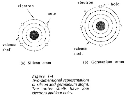
The atoms represented in Fig. 1-4 are those of two important Introduction to Semiconductor materials, silicon (Si) and germanium (Ge). It is seen that each of these atoms has four electrons in a valence shell that can contain a maximum of eight. Thus, the valence shells have four electrons and four holes. A hole is defined as an absence of an electron in a shell where one could exist. Even though the valence shells of silicon and germanium have four holes, both types of atoms are electrically neutral because the total number of orbiting (negatively charged) electrons equals the total number of (positively charged) protons in the nucleus.
The closer an electron is to the nucleus, the stronger are the forces that bind it. Each shell has an energy level associated with it that represents the amount of energy required to extract an electron from the atom. Since the electrons in the valence shell are farthest from the nucleus, they require the least amount of energy to extract them, [see Fig 1-5(a)]. Conversely, those electrons closest to the nucleus require the greatest energy application to extract them from the atom.
The energy levels of the orbiting electrons are measured in electron volts (eV). An electron volt is defined as the amount of energy required to move one electron through a voltage difference of one volt.
Energy Band Diagram of Semiconductor:
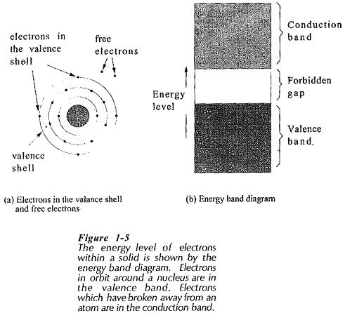
So far, the discussion has concerned a system of electrons in one isolated atom. The electrons of an isolated atom are acted upon only by the forces within that atom. However, when atoms are brought closer together, as In a solid, the electrons come under the influence of forces from other atoms. Under these circumstances, the energy levels that may be occupied by electrons merge into bands of energy levels. Within any given material there are two distinct energy bands in which electrons may exist; the valence band and the conduction band. Separating these two bands is an energy gap, termed the forbidden gap, in which no electrons can normally exist. The valence band, conduction band, and forbidden gap are shown diagrammatically in Fig. 1-5(b).
Electrons within the conduction band have become disconnected from atoms and are drifting around within the material. Conduction band electrons may be easily moved by the application of relatively small amounts of energy. Much larger amounts of energy must be applied to move an electron in the valence band. Electrons in the valence band are usually in orbit around a nucleus. For any given type of Introduction to Semiconductor Materials, the forbidden gap may be large, small, or nonexistent. The distinction between conductors, insulators, and semiconductors is largely concerned with the relative widths of the forbidden gap.
It is important to note that the energy band diagram is simply a graphic representation of the energy levels associated with electrons. To repeat; those electrons in the valence band are actually in orbit around the nucleus of an atom; those in the conduction band are drifting in the spaces between atoms.