Optoelectronics Devices Interview Questions and Answers:
1.What are photonic devices?
Ans. Photonic devices are those in which the basic particle of light (the photone) plays an important role. Photodetectors, solar cells and LASERS etc, are photonic devices.
2. What is photoelectric effect?
Ans. Photoelectric effect is the relationship between collection of light energy and reflection of electrons from a metal.
3. How wavelength and energy of a photon are related?
Ans. Wavelength, λ = 1.24/Energy, E in micrometre.
4. What is luminescence?
Ans. When a system absorbs energy in some form or the other, it may be partly re-emitted as radiation. This phenomenon is called luminescence. Luminescence is the general property of light emission. This phenomenon may occur in solids (crystals or glasses) as well as in liquids and gases.
5. What is electroluminescence?
Ans. When excitation occurs due to introduction of current into the sample, the resulting luminescence is called the electroluminescence. There arc two mechanisms for production of electroluminescence. One mechanism is photoemission in the act of electron-hole recombination. LEDs and P-N junction diodes are examples of this phenomenon. The second mechanism for electroluminescence is photoemission following electron impact excitation of an activator atom. This process has been observed in ZnS : Cu.
6. What is photoluminescence?
Ans. When carriers are excited by photon absorption, the radiation resulting from the recombination of the excited carriers is called the photoluminescence. One of the most common examples of photoluminescence is the fluorescent lamp.
7. What is cathodoluminescence?
Ans. If the excited carriers are produced by high-energy electron bombardment of the material, the mechanism is called the cathodoluminescence. This principle is used in cathode ray tube (CRT). oscilloscope and other visual display systems.
8. What is photoconductivity?
Ans. When the excess carriers are generated in a semiconductor by optical luminescence, the resulting conductivity is called photoconductivity. This is an important effect, with usual applications in the analysis of semiconductor materials and in the operation of different types of devices.
9. What is photoconductor gain?
Ans. Photoconductor gain can be defined as the ratio of the rate at which charge is collected by the contacts to the rate at which charge is created within the photoconductor.
10. What is the concept of photoconductivity?
Ans. When excess electrons and holes are produced in a semiconductor, there is a corresponding increase in conductivity of a sample as indicated by the following equation
Conductivity of semiconductor, σ = J/E = e(pμh + nμe)
When the excess carriers in a semiconductor are due to optical luminescence, the resulting conductivity is called photoconductivity.
11. What is photocurrent?
Ans. Electric current produced due to photoelectric effect is called the photocurrent.
12. What are photodetectors?
Ans. Photodetectors are the semiconductor devices that can detect optical signals through electronic processes.
13. Enlist the three electronic processes involved in photodetection.
Ans. Three electronic processes involved in photodetection are
(i) carrier generation by incident light (ii) carrier transport and/or multiplication and (iii) interaction of current with the external circuit to give the output signal.
13. Name some devices used for photodetection.
Ans. The best known devices used for photodetection are LDRs, photodiodes and phototransistors.
14. What is “dark current” of a photodiode?
Ans. The dark current is the current that exists when no light is incident.
15. State the working principle of photodiode.
Ans. Photodiode is a two-terminal semiconductor P-N junction device and is designed to operate with reverse bias. When light energy bombards a P-N junction, it dislodges valence electrons. The more light striking the junction, the larger the reverse current in a diode. It is due to generation of more and more charge carriers with the increase in level of illumination. This is the working principle of photodiode.
16. How the current is reduced to zero in a photodiode?
Ans. The reverse saturation current I0 flowing through a photodiode is reduced to zero by applying a forward bias voltage of magnitude equal to barrier potential.
17. What is PIN photodiode?
Ans. PIN photodiode consists of a P-region and N-region separated by an intrinsic region where width of intrinsic region is much larger than the space charge width of an ordinary PN junction.
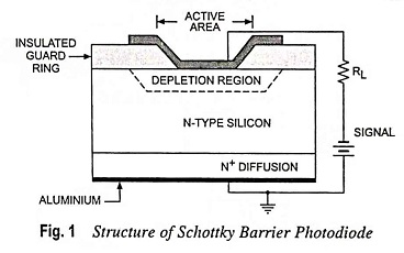
18. Draw the structure of Schottky-barrier photodiode.
Ans. The structure of Schottky-barrier photodiodes is shown in Fig. 1.
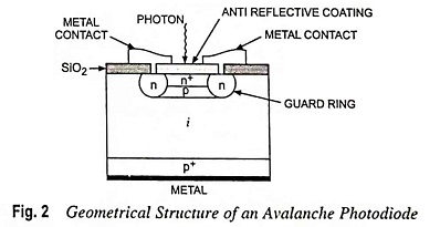
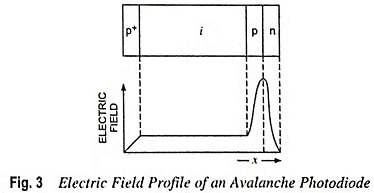
19. Draw the geometrical structure of an Avalanche photodiode and the electric field profile.
Ans. Geometrical structure and electric field profile of an Avalanche photodiode are shown in Figs. 2 and 3 respectively.
20. How does avalanche photodiode differ from PIN photodiode?
Ans. The avalanche photodiode is similar to PIN photodiode except that it is operated at high reverse-bias voltages so that impact ionization occurs.
21. Differentiate between photodiodes and phototransistors.
Ans. Photodiode is a two-terminal semiconductor P-N junction device and is designed to operate with reverse bias. It operates when light falls on its depletion layer.
Phototransistor is similar to an ordinary BJT except that no base terminal is provided. Instead of base current, the input to the transistor is in the form of light.
The main difference between a phototransistor and a photodiode is the current gain hfe or βdc. The same amount of light striking both devices produces βdc times more current in a phototransistor than in a photodiode. The increased sensitivity of a phototransistor is a big advantage over a photodiode. However, photodiodes are the faster of the two. A photodiode has typical output currents in microamperes and can switch on or off in nanoseconds while the phototransistor has typical output currents in milliamperes but switches on or off in microseconds.
22. Define sensitivity of a phototransistor.
Ans. Photosensitivity of a phototransistor is the ability of the phototransistor to provide the internal current multiplication in order to generate a large output signal. Higher the photosensitivity of phototransistor more amplification of the signal will be provided by the phototransistor.
23. What are photovoltaic or solar cells?
Ans. Photovoltaic or solar cells are semiconductor junction devices used to convert radiation energy into electrical energy. These cells generate a voltage proportional to electromagnetic radiation intensity and are called the photovoltaic cells because of their voltage generating capability.
24. How the main drawback of low sensitivity of vacuum type photocells has been overcome in gas filled photocells.
Ans. The main drawback of low sensitivity of vacuum type photocells has been overcome to some extent by increasing the number of electrons produced at the cathode by a gas discharge.
25. What is the disadvantage of multiplier phototubes?
Ans. The disadvantage of multiplier phototubes is that they are large in size and expensive in cost and require high voltage (between 500 V and 5,000 V) for their operation.
26. What is the main drawback of the photoconductive cells?
Ans. The major drawback of the photoconductive cells is that temperature variations cause substantial variation in resistance for a particular light intensity.
27. What is LED?
Ans. Light-emitting diode (LED) is the best known of all optoelectronic devices, which emits a fairly narrow bandwidth of visible (usually red, orange, yellow or green) or invisible (infrared) light when its internal diode junction is stimulated by a forward electric current/voltage (power).
28. What is radiative recombination in LED?
Ans. Whenever LED is forward biased, a forward current starts flowing through it. This current flows because of electrons supplied by the battery. The electrons supplied by the battery are free electrons and they reside in the conduction band. The energy level of conduction band is higher than that of valence band. These electrons recombine with holes to become valence electrons and come to a lower energy level. While coming back to the valence band, they give up the excess heat in the form of light. This process is called recombination in LED because of which light emits in LED.
29. What precautions are required to be observed in the use of LEDs?
Ans. LEDs should neither be reverse biased nor operated near their maximum current rating. The leads of a LED should never be bent closer than about 2 mm from the encapsulation.
30. State differences between LED and photodiodes.
Ans. Photodiode is a two-terminal semiconductor P-N device and is designed to operate with reverse bias. It works when light falls on depletion layer of P-N junction of photodiode. Photodiode is a photovoltaic device as well as photoconductive device. When it is operated with a reverse bias, it is photoconductive device and when operated without the reverse bias, it is a photovoltaic device.
LED stands for light-emitting diode. It emits a fairly narrow bandwidth of visible (usually red, orange, yellow or green) or invisible (infrared) light when its internal diode junction is stimulated by a forward electric current/voltage (power). The operation of LED is based on the phenomenon of electroluminescent, which is the emission of light from a semiconductor under the influence of electric field.
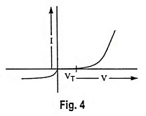
31. Sketch the terminal current-voltage characteristic of Light-emitting diode under forward and reverse biased conditions.
Ans. The terminal current-voltage characteristic of the LED under forward and reversed biased conditions is shown in Fig. 4.
32. Draw the V-I characteristics of GaAs and explain the significance of negative resistance.
Ans. V-I characteristics of GaAs are shown in Fig. 5.
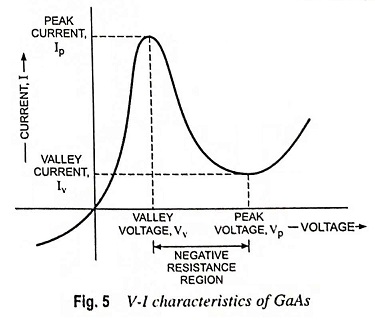
Negative resistance is a property of circuits/devices in which an increase in voltage across the device/circuit causes decrease in electric current through it. It develops power and finds applications in microwave amplifiers and oscillators and switching circuits.
33. Why LCDs are not operated from ac supply of frequency lower than 25 Hz and higher than 50 Hz?
Ans. If the frequency of supply to LCDs is lower than 25 Hz, a visible flicker would be produced and if it exceeds 50 Hz, the current drawn will be more.
34. How are LCD displays advantageous over LED displays?
Ans. The LCDs have the distinct advantage of having low power consumption than the LEDs. It is typically of the order of micro-watts for the display in comparison to the some order of mW for LEDs. Other advantages are lower cost and good contrast.
35. What are the drawbacks of LCDs?
Ans. The main drawbacks of LCDs are additional requirement of light source, limited temperature range of operation (0-60°C), poor reliability, short operating life, poor visibility in low ambient lighting, slow speed and the need for an ac drive.
36. What for does LASER stand?
Ans. LASER stands for light amplification by stimulated emission of radiation.
37. List the advantages of laser devices.
Ans. Laser devices are small in size, highly efficient, operate at low power inputs and their outputs are adjustable by varying the junction currents.
38. What are heterojunction lasers?
Ans. Heterojunction lasers are the multiple layer PN junction lasers with more than one junction and can provide still greater efficiencies and more power.
39. Why II-VI compounds are not used for the fabrication of semiconductor lasers though they are generally very efficient light emitters?
Ans. Because junctions are difficult to form.
40. Why semiconductors with indirect band gaps are not used for the fabrication of semiconductor lasers?
Ans. Because semiconductors with indirect band gaps are not sufficiently efficient light emitters for practical laser fabrication.
41. What is an optocoupler?
Ans. Optocoupler is a device that contains an infrared LED and a photodetector (such as a photodiode, phototransistor, Darlington pair, SCR or Triac) combined in a package.
42. How an optocoupling efficiency of an optocoupler device is expressed?
Ans. The optocoupling efficiency of an optocoupler may be specified by the output-to-input current transfer ratio (CTR). It may also be expressed as a ratio of output current IC (measured at the collector terminal of the phototransistor), to the input current IF flowing into the LED i.e., CTR = IC/IF.
43. Nixie tube display is based on what principle?
Ans. The working principle of Nixie tube is based on the fact that when an electric current is passed through a gas, it breaks down and produces a glow at that location. When negative voltage is applied to any cathode, the glow is produced and the corresponding numeral is displayed. The color of display depends upon the gas used.
44. Where is Nixie tube used?
Ans. Indicators, small, medium and large displays, small group viewing.
45. What are the display devices used in digital instruments?
Ans. LEDs and LCDs.