Oxidation in IC Fabrication:
Oxidation in IC Fabrication is very important process. In one line, oxidation can be explained as the production of SiO2 using the thermal growth technique. Some of the important uses of SiO2 are as follows.
- In bipolar and MOS transistors, it isolates one device from other.
- It provides surface passivation.
- It acts as a barrier or mask against the diffusion or the implantation of impurity dopant in substrate.
- In MOS devices, it acts as a component.
- It serves as a dielectric isolation between multilevel inter connect layers.
There are different techniques of forming SiO2 layer.
- Thermal oxidation .This is the basic process used in IC fabrication. When the charge density level at the interface of silicon and oxide is required low, this technique is used.
- Wet anodization
- Vapour phase oxidation. This process is also known as chemical vapour deposition. In multilevel structures, the SiO2 layer is formed on the top of the metal layer using vapour phase oxidation process.
- Plasma oxidation
Oxidation Techniques:
The selection of Oxidation in IC Fabrication technique to be used depends on oxide properties and the thickness of the oxide layer required. For thin oxides which require low charge at interface, the oxides are grown in a dry oxygen. Wet and dry oxidation process is preferred when sodium ion contamination is concerned. For thick oxides, steam is used at high pressure with relatively moderate temperatures. Let us study the most common process used in IC fabrication, Wet and dry thermal oxidation. The chemical reaction involved in this technique are
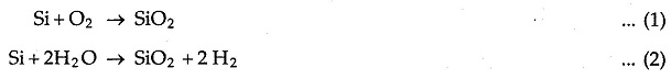
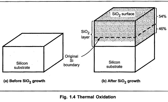
Equation (1) indicates reaction of silicon with oxygen, which is a dry oxidation. Equation (2) indicates reaction of silicon with water vapour or steam, which is wet oxidation. Using thermal oxidation, the oxygen diffuses through the oxide to the boundary of Si-SiO2. The reaction takes place at the boundary of Si-SiO2. After the completion of the oxide growth, almost 46% of the oxide layer piereces within the original substrate, while 54% of the remaining layer remains on the top of it as shown in the Fig. 1.4.
The silicon wafers are arranged in a quartz boat. Then the boat with support is inserted into quartz furnace. The temperature of the furnace lies in the range of 950°C to 1250°C and using proper control system, the temperature is kept constant to about ± 1/2°C. Then silicon wafers are exposed to gas containing O2 and or H2O. Following the chemical reactions stated earlier. An uniform depth and composition layer depends on the parameters such as growth time, temperature, pressure, O2 gas concentration etc.
Basically an Oxidation in IC Fabrication is high temperature process. Due to the oxidation process, the layer departs from its original location. To overcome this undesired result, the oxidation process is carried out at low temperatures. But this increases the growth time. To overcome this, pressure is increased because an increase by 1 atm pressure decrease temperature by 20°C for same growth rate. Thus high pressure oxidations with pressures upto 25 atm are used in the industrial applications at the temperatures in the range of 700 to 900°C.
Initially the oxide grow formation rate is very fast and then gradually it slows down as oxygen atoms have to diffuse through the oxide to reach the interface between silicon substrate and SiO2. As compared to dry oxidation process, wet oxidation process is faster at a given temperature. Typically to grow 1 μm thick oxide layer, dry oxidation process takes 2 hour 30 minutes while wet oxidation takes only 1 hour and 30 minutes. Event hough the wet oxidation process is time saving, it has a drawback of higher impurity contents of the oxides. Generally MOS ICs require a very pure oxide for reliable performance. For this purpose specially dry oxidation process is preferred.
For VLSI, the thin oxides of 20 to 200 A° are in demand. The growth rate for such thin oxide layers are very small. With low temperatures and pressures growth rate reduces. For such very thin oxide layers special techniques are applied. The oxide layers of 30 to 300 A° thick are grown at pressures of 0.2 to 2 Torr. In other technique, for a very thin oxide layer initially temperature is controlled at 1000°C typically, the growth is carried out with O2 – HCI agent and then heat treatment with N2, O2 and HCI is employed at 1250°C to work out desired thickness. By using low temperatures (750°C) and high pressures (10 atm) in combination, a 300A° thick layer can be grown in 30 minutes with this another special technique.
Oxide Properties:
For reliable performances of the devices, it is necessary to have a very pure oxide. To carry out the oxidation process successfully, it is necessary to study different properties of oxides.
1) Masking properties of 1250°CSiO2.
A silicon dioxide acts as a barrier or mask against the diffusion of dopant atoms. Due to ion implantation and chemical diffusion, the dopant atoms gather at the surface of the oxide or near the surface. So the utmost precaution must be taken during the diffusion of axide, such that the dopant atoms do not diffuse through the oxide. This can be achieved by controlling the diffusion in oxide slower as compared to that in silicon. At a particular temperature and pressure, the oxide thickness can be measured experimentally which is essential to avoid the inversion of the lightly doped silicon substrate. In typical devices, the oxide thickness required for the masking purpose is 0.5 to 0.7 μm. The masking property can be realized only when the oxide is partially converted into the silica. For different dopant atoms, the diffusion constants in silicon dioxide are different. These are dependent on the structure and concentration of SiO2. For n-type, the common impurities are phosphorous (P), Antimony (Si), Arsenic (As), while for p-type Borone (B) is the common impurity.
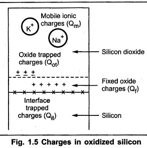
2) Oxide Charges:
The thermally oxidized silicon consists different types of charges. There exists a transition region at the silicon silicondioxide interface. At this interface some of the charges are found. These charges induce opposite polarity in the silicon substrate, changing the characteristics of MOS devices. At interface, the silicon dioxide layer departs from the ideal charge neutrality expected. There are three types of the charges namely :
- Fixed oxide charge (Qf)
- Mobile ionic charge (Qm)
- Oxide trapped charge (Qot)
The fixed oxide charge Qf is usually positive. This can not be charged or discharged. It is not allowed beyond 30A° of Si — SiO2 interface. Depending upon oxidation and annealing conditions, its density ranges from 1010 cm-2 to 1012 cm-2.
The mobile ionic charge Qm is positive most of the times. The alkali ions such as sodium, potassium are referred as mobile ion charge. But the negative ions and heavy metals are also referred as ionic charges. The density of Qm ranges from 1010 cm-2 to 1012 cm-2. The radi of ionic charges are more and also their mobility is very low.
The oxide trapped charge Qot is either positive or negative. It arises from either holes or electrons trapped in the oxide. The main cause of Qot is the defects in the oxides. Also due to avalanche injection, ionizing radiations and high currents in the oxides, Qot may be induced. The density of Qot ranges from 109 cm-2 to 1013 cm-2 . In addition to these charges, there is an interface trapped charge Qit.
All these charges are calculated using capacitance voltage (C–V) analysis technique.
3) Oxide stress:
During the thermal oxidation of silicon, at the surface, SiO2 is observed in a state of compression. This is clearly indicated by thermally wrapped silicon dioxide. The complex stress distribution takes place due to the cut in the oxides. Thus there is a danger of high stress levels formation at the discontinuities.
The stress can be relieved by using stress-relief mechanisms. Typically oxidation at 950°C or below, the stress is of the order of 7 x 10⁹ dyne/cm2. At room temperature, the stress is found to be 3 x 10⁹ dyne/cm2.
Oxidation Induced Defects:
1) Oxidation Induced Stacking Faults :
Stacking faults are produced on <111> planes due to thermal oxidation of silicon. The stacking faults are structural defects in the silicon lattice which are of extrinsic type and are limited by partial dislocations. There is coalescence of excess silicon atoms in the silicon lattice on nucleation site. This is called as growth mechanism. The growth mechanism involves defects formed during growth of a crystal, surface mechanical damage present before oxidation, chemical contamination and saucer pits or hillocks.
Due to process of Oxidation in IC Fabrication the excess interstitial silicon is present near the Si – SiO2 interface. A small part of these silicon atoms flow into the bulk silicon. Growth rate depends upon the silicon interstitial supersaturation in silicon. Stacking faults create some problems like degraded junction characteristics and increased reverse current in MOS structures.
The growth of oxidation induced stacking faults is a function of orientation of substrate, conductivity type and the defect nuclei present. Growth rate is greater in <100> than in <111> substrates.
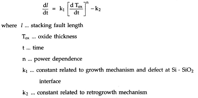
The length of stacking fault is a function of oxidation temperature. For lower oxidation temperature, less stacking faults are grown. For oxidation temperature less than 950°C, the stacking faults formation is suppressed completely.
Formation of the stacking fault length depends on rate of oxidation which is given by
2) Oxide Isolation Defects :
Silicon is treched before oxidation, to produce planar surface. It produces recessed oxides. In such recessed oxides stress along the edge of an oxidizing area causes defects in silicon. These defects cause increased leakage in nearby devices. Growing oxides generate the stress. This stress should be relieved without damaging the silicon. Sufficiently high oxidation temperature relieves the stress in oxides by viscous flow to make the oxide isolation to defects lesser. It can also be achieved by growing a selective oxide without first trenching the silicon. It is also seen that there is less oxidation in the stressed region which is covered by nitride mask.