True RMS Voltmeter:
True RMS Voltmeter – Complex waveform are most accurately measured with an rms voltmeter. This instrument produces a meter indication by sensing waveform heating power, which is proportional to the square of the rms value of the voltage. This heating power can be measured by amplifying and feeding it to a thermocouple, whose output voltages is then proportional to the Erms.
However, thermocouples are non-linear devices. This difficulty can be overcome in some instruments by placing two thermocouples in the same thermal environment.
Figure 4.25 shows a block diagram of a true rms responding voltmeter.
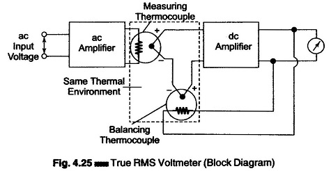
The effect of non-linear behavior of the thermocouple in the input circuit (measuring thermocouple) is cancelled by similar non-linear effects of the thermocouple in the feedback circuit (balancing thermocouple). The two couples form part of a bridge in the input circuit of a dc amplifier.
The unknown ac voltage is amplified and applied to the heating element of the measuring thermocouple. The application of heat produces an output voltage that upsets the balance of the bridge.
The dc amplifier amplifies the unbalanced voltage; this voltage is fed back to the heating element of the balancing thermocouple, which heats the thermocouple, so that the bridge is balanced again, i.e. the outputs of both the thermocouples are the same. At this instant, the ac current in the input thermocouple is equal to the dc current in the heating element of the feedback thermocouple. This dc current is therefore directly proportional to the effective or rms value of the input voltage, and is indicated by the meter in the output circuit of the dc amplifier. If the peak amplitude of the ac signal does not exceed the dynamic range of the ac amplifier, the true rms value of the ac signal can be measured independently.
True RMS Meter:
There exists a fundamental difference between the readings on a normal ac meter and on a true rms meter. The first uses a D’ Arsonval movement with a full or half wave rectifier, and averages the values of the instantaneous rectified current.
The rms meter, however, averages the squares of the instantaneous current values (proportional, for example, to the instantaneous heating effect). The scale of the true rms meter is calibrated in terms of the square roots of the indicated current values. The resulting reading is therefore the square root of the average of the squared instantaneous input values, which is the rms value of the measured alternating current.
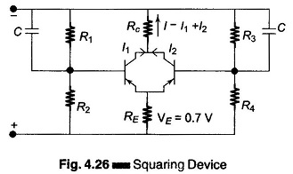
A true rms meter is always a combination of a normal mean value indicating meter and a squaring device whose output at any instant is proportional to the instantaneous squared input.
It can be shown that the ac component of the voltage developed across the common collector resistors of two transistors that are connected in parallel, and between the bases of which a small ac voltage is applied, is proportional to the square of the applied input voltage.
The basic circuit of Fig. 4.26 employing two transistors is completed by a bridge arrangement in which the dc component is cancelled out. This bridge arrangement is given in Fig. 4.27.
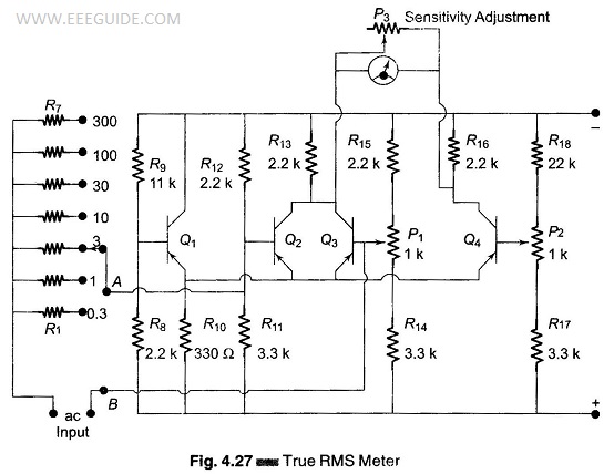
One side of the bridge consists of two parallel connected transistors Q2 and Q3, and a common collector resistor R13. The side of the bridge, employing P1 for bias setting, is the basic squaring circuit. The other side of the bridge is made of transistor Q4 (whose base is biased by means of potentiometer P2 and collector resistance R16.)
Potentiometer P1, base bias balance of the squaring circuit, must be adjusted for symmetrical operation of transistors Q2 and Q3. To do this, the polarity of a small dc input voltage applied to terminals A and B (bases of Q2 and Q3) has to be reversed, and the reading of the output meter must be the same for both input polarities.
Potentiometer P2 must be set so that for zero input signal (terminals A and B short-circuited), the bridge is balanced and the meter reads zero. The balance condition is reached if the voltage drop across the collector resistance R13 of Q2 – Q3, and collector resistance R16 of Q4, are equal.
Transistor Q1 is used to improve the temperature stability of the whole circuit, which is basically obtained by the emitter resistance R10. Optimum temperature compensation is obtained if the voltage drop across the emitter resistance for no signal is 0.7 V for silicon transistor.
The low current through Q2, Q3, Q4 requires a large emitter resistance value to fulfil the condition for compensation. Therefore, another transistor, Q1 has been added to compensate for the temperature changes of Q2 and Q3.
The bias on this transistor has to be adjusted by selecting appropriate values of R8 and R9 so that the voltage drop across R10 in the balanced condition is 0.7 V for silicon transistor.
The input of the squaring devices (AB) is connected to a voltage divider that is calibrated in seven ranges, namely 0.3, 1, 3, 10, 30, 100, and 300 volts.