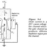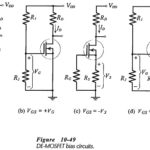
MOSFET Biasing Circuits
MOSFET Biasing Circuits: DE-MOSFET Bias Circuits - DE-MOSFET bias circuits are similar to JFET bias circuits. Any of the FET bias circuits already discussed can be used to produce a…
Continue Reading
MOSFET Biasing Circuits