Clock Generator 8284A:
During fetch and execute instructions, the 8086 and 8088 processors require clock pulse which has about 10 ns rise and fall times. The logic 0 level of the clock is 0.5 V to 0.6 V, logic-1 level is about 3.9 V to 5 V and the clock duty cycle is about 33%. The 8086 processor has no clock generator inside the chip. So, an external clock generator IC must be connected with the processor. The 8284A is a clock generator IC and it is a supporting component to the 8086/8088 processors. The 8284A IC has the following features or additional basic functions such as clock generation, RESET synchronization, READY synchronization, and a TTL level peripheral clock signal. The operation of 8284A IC has been explained in this section.
Operation of 8284A Clock Generator
The internal logic of the 8284A clock generator is depicted in Fig. 5.32. The upper half of the logic diagram represents the clock and reset synchronization section of the 8284A clock generator. It is depicted in Fig. 5.32 that the crystal oscillator has 2 inputs: X1 and X2. When a crystal is connected to X1 and X2 terminals, the oscillator generates a square-wave signal and its frequency is same as the crystal frequency.
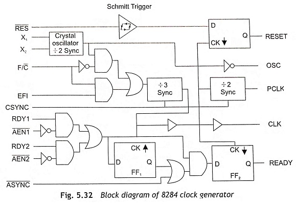
The output square-wave signal is fed to an AND gate and it is inverted by using an inverting buffer to generate the OSC output signal. The OSC signal can be used as an EFI input to other 8284A clock generators. When F/C̅ is a logic 0, the output of the AND gate is fed to divide-by-3 synchronous counters. If F/C̅ is a logic 1 then EFI is steered through to the counter.
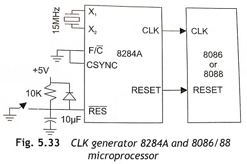
The output of the divide-by-3 synchronous counters generates the ready signal for synchronization. The CLK signal is buffered before output from the clock generator. Another divide-by-2 synchronous counter generates the PCLK signal to the 8086/8088 microprocessor. When the output of the first ÷3 synchronous counters is fed to the second ÷2 synchronous counters, the two cascaded counters generate ÷6 outputs at PCLK. Figure 5.33 shows the connection between 8284A and the 8086/8088 processor. Usually, F/C̅ and CSYNC are connected with ground to select the crystal oscillator. Then a 15 MHz crystal generates the normal 5 MHz CLK clock signal and a 2.5 MHz peripheral clock signal PCLK.
The reset section of the 8284A consists of Schmitt trigger buffered and a D type flip-flop. The D flip-flop ensures that the timing requirements of the 8086/8088 RESET input are met. This circuit applies the RESET output signal of clock generator is fed to the microprocessor as shown in Fig. 5.32, and it is active on the negative edge the clocks. Hence, the reset section meets the timing requirements of the 8086/8088 microprocessor.
Pin Functions of 8284A Clock Generator
The 8284A is an 18 pin IC which is specifically designed for 8086/8088 microprocessors. The pin diagram of the chip is shown in Fig. 5.34. In this section, the functions of pins are explained.
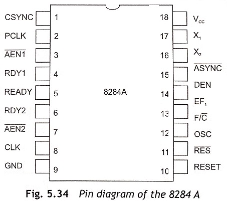
X1 and X2 Crystal Inputs These pins are connected to an external crystal which is used as a clock frequency source of the clock generator. The external crystal clock frequency will be about three times the required frequency. If the required frequency is 5 MHz, the crystal frequency will be 15 MHz.
CLK CLK is an output pin that provides the clock (CLK) signal which is used as input signal to the 8086/8088 microprocessor system. The CLK pin has an output signal with 33% duty cycle as required by the 8086/8088.
EFI (External Frequency Input) This is an alternate clock input when F/C̅ pin is pulled high. The externally generated clock signal is supplied to EFI whenever the F/C̅ pin is high.
PCLK (Peripheral Clock) This is a clock output signal that is one sixth of the crystal. PLCK is half of the clock frequency and has a 50% duty cycle. The PCLK output signal can be used as a clock signal to the peripheral equipment’s in 8086/8088 system.
OSC (Oscillator Output) This is an oscillator-output signal which is running at crystal or EFI frequency. This signal can be used to provide clock signal at EFI to the other 8284 clock generators in some multiple processor system.
F/C̅ (Frequency/Crystal) The voltage on this pin determines the clocking source for the 8284A. If this input pin is high, an external clock at EFI is selected. While it is low, the internal crystal oscillator provides the clock frequency signal.
CSYNC (Clock Synchronization) This pin is used for synchronization of clock signals in a multiprocessor system where all processors receive the clock at EFI. If the internal crystal oscillator is used, this pin must be grounded. When CSYNC is high, the 8284A clock generator stops working.
R̅E̅S̅ (Reset Input) To reset the 8086 processor, 8284A clock generator should send the RESET signal. Generally, this pin is connected to an RC network for generating RESET signal at power on.
RESET (Reset Output) This signal is connected to the 8086/8088 RESETs input pin. The RESET signal must be synchronized with the clock.
RDY1 , RDY2 The slow memory or I/O devices can request for extension of bus cycles using RDY1 or RDY2 pins. These two wait-state ready inputs are provided to support a 8086/8088-based system.
READY The READY output pin connects to the 8086 READY input which enables the bus cycle period insertion between T3 and T4. The 8086 READY signal must be synchronized with the RDY1 and RDY2 inputs.
A̅S̅Y̅N̅C̅ (Ready Synchronization Select) This input pin is used to select either one or two stages of synchronization for the RDY1 and RDY2 inputs. If it is low, one level is selected. When it is high, two levels of synchronization are selected.
A̅E̅N̅1, A̅E̅N̅2 Two ready inputs RDY1, RDY2 have been provided in the 8284A to support the multibus system. The 8086 CPU may be connected to two separate system buses, on which data transfer takes place. The memory or I/O devices of any system bus may like to insert wait states. Hence, each system bus should have its own ready line. A̅E̅N̅1 and A̅E̅N̅2 are provided to arbitrate bus priorities whenever RDY1 and RD2 are active. The 8284A responds to RDY1 when A̅E̅N̅1 is low. In the same way, clock generator responds to RDY2 if A̅E̅N̅2 is low.
VCC (Power Supply Input) This pin is connected to + 5 V ± 10%.
GND (Ground) This pin must be grounded.