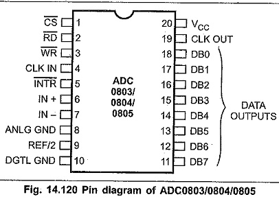
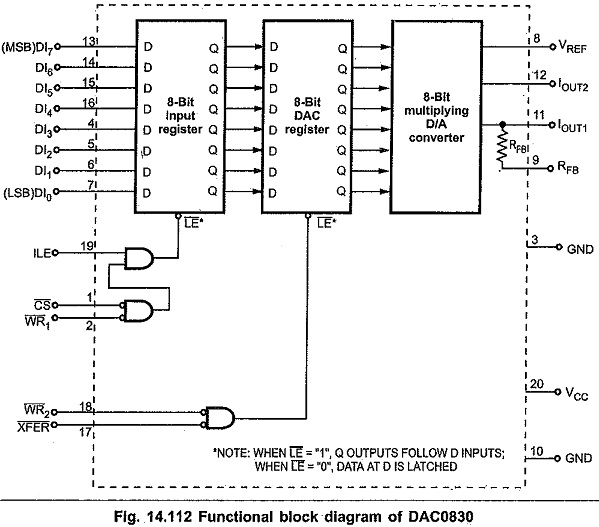
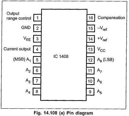
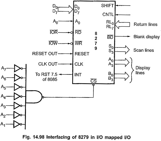
Sample and Hold Circuit
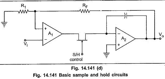
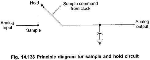
Sample and Hold Circuit: Four basic sample and hold circuit are shown in Fig. 14.141. In these circuits a JFET is used as switch. During the sampling time the JFET switch is turned on, and…
Comments Off on Sample and Hold Circuit
August 22, 2018