Sample and Hold IC:
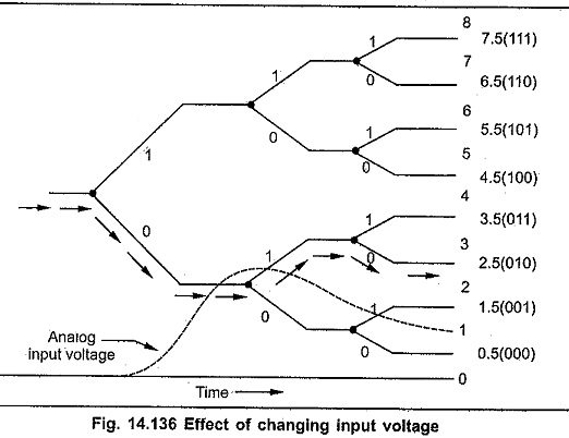
Sample and Hold IC – For accurate analog to digital conversion the analog input voltage should be held constant during the conversion cycle. If the analog input voltage changes by more than ± 1/2 LSB an error can occur in the digital output code. To illustrate the effect of a changing analog input voltage on the conversion processor, let us consider a situation of a successive approximation ADC with an analog input voltage that is initially zero, but there happen to be a large change in voltage amplitude occurring during the conversion process. Fig. 14.136 shows the changing input voltage and its effect on the successive approximation conversion process.
As shown in Fig. 14.136 analog input voltage at start of conversion process is zero volts and at the end of conversion process it is near to 1.5 volts, and the conversion process result is 0102, i.e. 2.5 V. This result does not corresponds to the analog voltage at the start of conversion or at the end of conversion. To minimise the occurrence of these errors it is necessary to hold the value of the analog input voltage constant during the conversion process. The Sample and Hold IC circuit does this task.
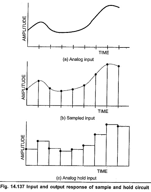
As its name implies, the Sample and Hold IC (S/H) circuit samples the value of the input signal in response to a sampling command and hold it at the output until arrival of the next command. It samples an analog input voltage in a very short period, generally in the range of 1 to 10 μs, and holds the sampled voltage level for an extended period, which can range from a few millisecond to several seconds. Fig. 14.137 shows input and output response of the Sample and Hold IC circuit.
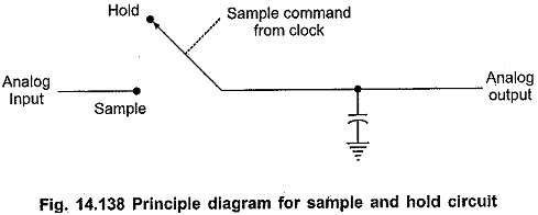
The Sample and Hold IC circuit uses to basic components analog switch and capacitor. The Fig. 14.138 shows the basic sample and hold circuit.
The circuit tracks the analog signal until the sample command causes the digital switch to isolate the capacitor from the signal, and the capacitor holds this analog voltage during A/D conversion.
Analog Switches:
JFET can be used as an analog switch. For this, the gate-source voltage VGS is restricted to two values : 0 V or a large negative voltage. The negative voltage must be equal to or more than VGS(OFF). When VGS is zero, the JFET operates in the ohmic region and JFET acts as a closed switch. When VGS is more negative than VGS(OFF), the JFET is cut off and the switch is open.
Shunt Switch:
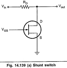
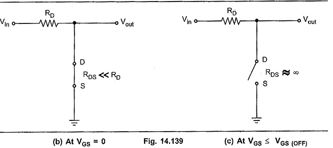
Fig. 14.139 shows JFET used as a shunt switch. The JFET is turned on and off by VGS. When VGS = 0 V, JFET acts as a closed switch and RDS is much less than RD. Due to the voltage divider action Vout is very small, approximately equal to 0 V. When VGS is more negative than VGS(OFF), the JFET acts as an open switch. Due to this Vout is equal to Vin.
Series Switch:
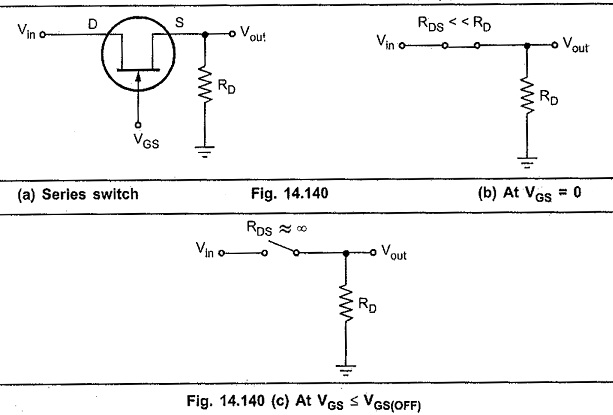
Fig. 14.140 shows JFET used as a series switch. When VGS = 0 V, the switch is closed and Vout equals Vin. When VGS is equal to or more negative than VGS(OFF), the JFET is open and Vout is approximately zero.
