Field Effect Transistors

MOSFET Construction and Characteristics

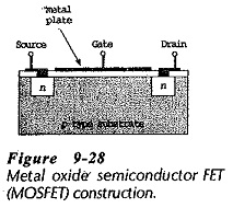
MOSFET Construction and Characteristics: Figure 9-28 shows the MOSFET Construction and Characteristics of a metal oxide semiconductor FET (MOSFET), also known as an insulated gate FET. Starting with a high-resistive p-type substrate, two blocks of heavily-doped n-type material are diffused into the substrate, and then the surface is coated with a layer of silicon dioxide. […]

MOSFET Construction and Characteristics Read More »

FET Amplification

FET Amplification: Consider the n-channel FET Amplification circuit in Fig. 9-26. Note that drain-source terminals are provided with a dc supply (VDD), connected via the drain resistor (R1). The gate-source junctions are reverse-biased by the gate voltage (VG). An ac signal generator (with voltage vf) is connected in series with the gate terminal. As already

FET Amplification Read More »

FET Datasheet Specifications

FET Datasheet Specifications: Maximum Ratings – A portion of a FET Datasheet Specifications is reproduced in Fig. 9-17. As with other device data sheets, a device type number and brief description is usually given at the start. Maximum ratings follow, and then the electrical characteristics are stated for specific bias conditions. From Fig. 9-17, the maximum drain-source

FET Datasheet Specifications Read More »

JFET Characteristics

JFET Characteristics: An n-channel JFET Characteristics block representation is shown in Fig. 9-6. With a drain-source voltage applied as illustrated, ID flows in the direction shown producing voltage drops along the channel. Consider the voltage drops from the source terminal (S) to points A, B. and C within the channel. Point A is positive with

JFET Characteristics Read More »

Scroll to Top