BJT Biasing Articles:
DC Load Line of BJT Biasing Circuit: The DC Load Line of BJT Biasing Circuit is a straight line drawn on the transistor output characteristics. For a common-emitter (CE) circuit, the load line is a graph of collector current (IC) versus … (Read More)
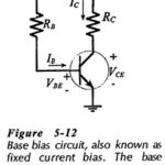
Base Bias in BJT: Circuit Operation and Analysis – The transistor bias arrangement shown in Fig. 5-12 is known as Base Bias in BJT and also as fixed current bias. The base current is a constant quantity determined by supply voltage … (Read More)
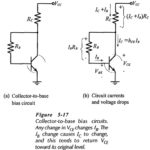
Collector to Base Bias Circuit: The Collector to Base Bias Circuit shown in Fig. 5-17(a) has the base resistor (RB) connected between the transistor collector and base terminals. As will be demonstrated, this circuit has significantly improved bias stability for hFE … (Read More)
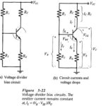
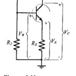
Voltage Divider Bias Circuit: Circuit Operation – Voltage Divider Bias Circuit, also known as emitter current bias, is the most stable of the three basic transistor bias circuits. A voltage divider bias circuit is shown in Fig. 5-22(a), and the current … (Read More)
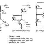
Comparison of Different Biasing Circuits: The Comparison of Different Biasing Circuits of the three basic bias circuits, it must be recalled that transistor manufacturers specify maximum and minimum hFE values for each transistor type number at various levels of collector current. Normally, … (Read More)
BJT Bias Circuit Troubleshooting: Voltage Measurement – When a BJT Bias Circuit Troubleshooting is constructed in a laboratory situation, the supply voltage (VCC) and the voltage levels at the transistor terminals (VC, VB and VE) should be measured with to the ground … (Read More)
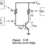
Bias Circuit Design: Bias Circuit Design can be amazingly simple. Usually, it is just a matter of determining the required voltage across each resistor and the appropriate current levels. Then, the resistor values are calculated by application of Ohm’s law. Designs usually … (Read More)
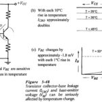
Bias Circuit Thermal Stability: VBE and ICBO Variations – Many transistor circuits are required to operate over a wide temperature range. So, another aspect of bias circuit stability is Bias Circuit Thermal Stability, or how stable IC and VCE remain when the … (Read More)
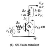
Biasing Transistor Switching Circuits: Direct-Coupled Switching Circuit – When a transistor is used as a Biasing Transistor Switching Circuits, it is either biased off to IC = 0, or biased on to its maximum collector current level. Figure 5-53 illustrates the … (Read More)