JFET Bias Circuit Design
JFET Bias Circuit Design: Design Approach - Design of JFET Bias Circuit Design is just as simple as design of BJT bias circuits. One major difference is that FET circuit…
Continue Reading
JFET Bias Circuit Design
JFET Bias Circuit Design: Design Approach - Design of JFET Bias Circuit Design is just as simple as design of BJT bias circuits. One major difference is that FET circuit…
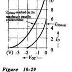
JFET Bias Circuit Troubleshooting: Voltage Measurement - JFET Bias Circuit Troubleshooting are similar to those for BJT bias circuits. The major difference is that there is only one junction in…
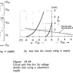
JFET Biasing Circuits: Use of Plus/Minus Supplies - When plus/minus supply voltages are to be used with a JFET Biasing Circuits, the gate terminal is usually grounded via RG, as…
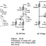
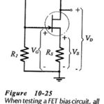
Basic JFET Biasing Circuits Comparison: The Basic JFET Biasing Circuits Comparison (gate bias, self-bias, and voltage divider bias) are similar in performance to the three basic BLIP bias circuits, (base…
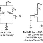
JFET Differential Amplifier - Circuit Diagram and its Workings: Many differential amplifiers are constructed with FETs because of the large impedance they present to the input signals—an exceptionally important property…
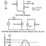
Fet Tuned Amplifier - Circuit Diagram and Frequency Response: Figure 18.11(a) depicts the circuit of an FET tuned amplifier. It uses a first-order JFET model for the 2N 5484 [IDSS…
Difference between JFET and MOSFET: The Difference between JFET and MOSFET are quite similar in their operating principles and in their electrical characteristics. However, they differ in some aspects, as…
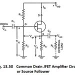
Common Drain JFET Amplifier or Source Follower: In the Common Drain JFET Amplifier circuit (also called the source follower), the output voltage is developed across source resistor RS. External load…