Diode Fabrication Process and Packaging
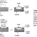
Diode Fabrication Process and Packaging: Alloy and Diffused Diodes - Two commonly used techniques for Diode Fabrication Process and Packaging are the alloy method and the diffusion method. To construct…
PN Junction Diode Interview Questions and Answers: 1. What is a P-N junction? Ans. The contact surface between the layers of P-type and N-type semiconductor pieces placed together so as to…
What is Real Diode? As already mentioned, an actual diode neither behaves as a perfect conductor when forward biased nor as a perfect insulator when reverse biased. When a diode…
Terminal Characteristics of Junction Diodes: The volt-ampere characteristic of a silicon junction diode is depicted in Fig. 7.14. The same Terminal Characteristics of Junction Diodes is depicted in Fig. 7.15…
IC Fabrication Articles: Processing of Semiconductor Materials: Preparation of Silicon and Germanium – Silicon is one of the commonest elements on earth. It occurs as silicon dioxide (SiO2) and as…
Integrated Circuits Fabrication Process: IC Types - An Integrated Circuits Fabrication Process consists of several interconnected transistors, resistors, etc., all contained in one small package with external connecting terminals. The…
Pin Diode Construction: The Pin Diode Construction consists of a narrow layer of p-type semiconductor separated from an equally narrow layer of n-type material by a somewhat thicker region of…
Impatt Diode Working: IMPATT Diode Working is a combination of delay involved in generating avalanche current multiplication, together with delay due to transit time through a drift space, provides the…