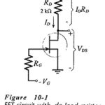
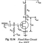
DC Load Line and Bias Point of FET Circuit.
DC Load Line and Bias Point of FET Circuit: The DC Load Line and Bias Point for a FET circuit is drawn upon the output characteristics of the device in…
DC Load Line for FET: The DC Load Line for FET circuit is drawn on the device output characteristics (or drain characteristics) in exactly the same way as for a…
DC Load Line of BJT Biasing Circuit: The DC Load Line of BJT Biasing Circuit is a straight line drawn on the transistor output characteristics. For a common-emitter (CE) circuit,…
DC Load Line Analysis of Semiconductor Diode: Figure 2-13(a) shows a DC Load Line Analysis of Semiconductor Diode in series with a 100 Ω resistance (R1) and a supply voltage (E).…
Transistor Load Line Analysis (DC and AC Load Line and Q Point): The concept of Transistor load line analysis is very important in understanding the working of a transistor. It…
Non Linear Wave Shaping Articles: What is Clipper Circuit? – Definition and Classification: Clipper Circuit is one which controls the shape of the waveform by removing or “clipping” off an…
Linear Applications of Op Amp Articles: Summing, Scaling and Averaging Amplifier: The most useful of the op-amp circuits employed in analog computers is the summing amplifier circuit. This circuit can…
HVDC Circuit Breakers - Construction and Working Principle: Light duty dc circuit breakers have been in use since long. However, there is lack of suitable circuit breakers for HVDC systems.…