Transistor Construction Techniques and Performance:
The following are Transistor Construction Techniques and Performance are as follows,
Current Gain:
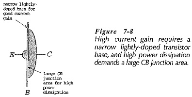
Good current gain requires that most charge carriers from the emitter pass rapidly to the collector. So, there should be little outflow of charge carriers via the base terminal, and there should be few carrier re-combinations within the base. These conditions dictate a very narrow, lightly doped, base, (see Fig. 7-8).
High Power:
Another Transistor Construction Techniques and Performance are High-power transistors must have large emitter-base surfaces to provide the required quantity of charge carriers. Large collector-base surfaces are also required to dissipate power without overheating the collector-base junction, (Fig. 7-8).
Frequency Response:
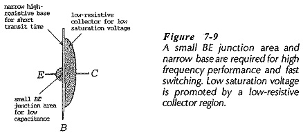
For the highest possible frequency response, the transistor base region must be very narrow to ensure a short transit time of charge carriers from emitter to collector, (see Fig. 7-9). Input capacitance must also be kept to a minimum, and this requires a small area emitter-base junction as, well as a highly-resistive (lightly doped) base region.
Because power transistors require large junction surfaces, and high-frequency performance demands small junction areas, there is a conflict in high-frequency power transistors. To keep the junction area to a minimum and still provide adequate charge-carrier emission, the emitter-base junction is usually in the form of a long thin zig-zag strip.
Switching Transistors:
Another Transistor Construction Techniques and Performance are Switching Transistors. Fast switching demands the same low junction capacitance required for good high-frequency performance. A switching transistor should have a low saturation voltage and a short storage time. For low saturation voltages, the collector region must have low resistivity, (Fig. 7-9). Short storage time requires fast recombination of charge carriers left in the depletion region at the collector-base junction. Fast recombination is assisted by additional doping of the collector with gold atoms.
Breakdown and Punch-Through:
The transistor collector-base junction is normally reverse biased, so the maximum collector voltage is limited by the junction reverse breakdown voltage. To achieve high breakdown voltages, either the collector or the base must be very lightly doped. If the base is more lightly doped than the collector, the collector-base depletion region penetrates deeply into the base. This will cause transistor breakdown by punch-through when it links with the emitter-base depletion region. To avoid punch through, the collector region close to the base is usually more lightly doped than the base. The collector-base depletion region then spreads into the collector, rather than into the base.