Vertical Deflection Circuit in TV:
The Vertical Deflection Circuit in TV include the vertical oscillator and amplifier for vertical scanning at 60 Hz and a similar horizontal arrangement for scanning at 15,750 Hz. For either scanning, the oscillator provides a deflection voltage at a frequency determined by its time constants and corrected by the appropriate sync pulses. This voltage is used to drive the corresponding output amplifier, which provides a current of the correct waveform, and at the right frequency, for the deflection coils. Magnetic deflection is always used for TV picture tubes and requires a few watts of power for the complete 90° or 110° (measured diagonally) deflection across the tube. Two pairs of Vertical Deflection Circuit in TV coils are used, one pair for each direction, mounted in a yoke around the neck of the picture tube, just past the electron gun.
This section is devoted to the Vertical Deflection Circuit in TV receiver but, before these can be discussed, it is necessary to look at the waveforms required and the means of producing them.
Sawtooth Deflection Waveform:
The scanning coils require a linear current change for gradually sweeping the beam from one edge of the screen to the other. This must be followed by a rapid (not necessarily linear) return to the original value for rapid retrace. The process must repeat at the correct frequency, and the average value must be zero to ensure that the picture is correctly centered. The waveform just described is in fact a sawtooth current; obtainable from a sawtooth voltage generator. It is shown in Figure 17-16a.
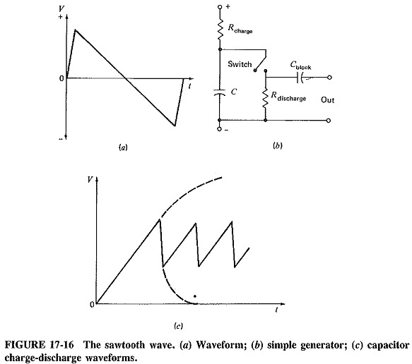
If a capacitor is allowed to charge through a resistance to some high voltage (solid line in Figure 17-16c), the voltage rise across it will at first be linear. As the voltage rises across the capacitor, so the remaining voltage to which it can charge is diminished, and the charging process slows down (dashed line in Figure 17-16c). The process is useful because it shows that linear voltage rise can be achieved if the charging process can be interrupted before its exponential portion. If, at this point, the capacitor is discharged through a resistor smaller than the charging one, a linear voltage drop will result (solid line in Figure 17-16c). Although linearity is not quite so important for the discharge, speed is important, so that the discharge process is not allowed to continue beyond its linear region, as shown in Figure 17-16c. If the ratio of charge time to discharge time is made about 8:1, we have the correct relationship for sweep and flyback of the vertical scanning waveform.
Figure 17-16b shows the simplest method of obtaining the charge/discharge sequence just described. Note that the charge process is not actually interrupted. The capacitor continues to charge (slowly) while it is being discharged, but this presents no problem. All that happens is that the discharge resistor is made slightly smaller to speed up discharge than it would have been if charge had been interrupted. To stop the slow charging during discharge would require a second switch synchronised with the first one, a needless complication. Note that Cblock in Figure 17-16b ensures that an ac sawtooth voltage is obtained from this circuit, being identical to Figure 17-16a.
Blocking Oscillator:
Having determined what waveform is required for scanning, and the basic process for obtaining it, we must now find a suitable switch. A multivibrator will fill the bill, but not really at a frequency as low as 60 Hz. The blocking oscillator, which, as shown in Figure 17-17a, uses an iron-cored transformer, is perfectly capable of operating at frequencies even lower than 60 Hz. It is almost invariably used as the vertical oscillator in TV receivers and is also sometimes used as the horizontal oscillator.
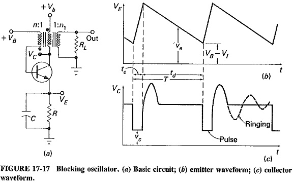
The blocking oscillator, unlike a multivibrator, uses only one amplifying device, with the transformer providing the necessary phase reversal (as indicated by the dots in Figure 17-17a). As a result, there cannot really be a bistable version of such a circuit, but monostable and astable versions are common. Like the corresponding multivibrator, the free-running blocking oscillator is capable of being synchronized. The circuit shown is an astable blocking oscillator. A careful look reveals its similarity to the Armstrong oscillator. Although the operation could be explained from that point of view, it is more common, and Probably easier, to understand the operation from a step-by-step, pulse-type treatment.
The blocking oscillator uses an iron-cored pulse transformer, with a turns ratio having a n : 1 voltage stepdown to the base, and a 1: n1 voltage stepup to RL. RL is the load resistor with the subsidiary function of damping out undesired oscillations. Such oscillations are likely to break out at the end of each collector pulse.
The circuit diagram shows the base winding returned to a positive voltage VB. It is evident that this oscillator must be free-running, since there is no potential present which could cut the base off permanently. Note that the circuit can be converted to a triggered or monostable blocking oscillator by the simple expedient of turning VB into a negative voltage. Trigger pulses are then required to make the circuit oscillate.
Assume, initially, that there is a voltage on C,νe, larger than VB – V1, where V1 is the cut-in base-to-emitter voltage. Such a situation is in fact shown at the beginning of the waveform in Figure 17-17b. Since this is the emitter-ground voltage of the transistor at that instant, the transistor is quite clearly OFF, and C is therefore discharging exponentially toward ground, with a time constant RC. When νe is reduced to equal VB – V1, the base starts to draw current, as does the collector, and regenerative action begins.
The increase (from an initial value of zero) in collector current lowers collector voltage, which in turn raises the base voltage. Still more collector current flows, resulting in a further drop in collector current. In practical circuits loop gain exceeds unity, so that regeneration takes place and the transistor is very quickly driven into saturation. (The base waveform, which is not shown here, has exactly the same appearance as the collector waveform of Figure 17-17c. It is inverted and scaled down by the factor n:1.)
The very short period of time just described marks the beginning of the collector output pulse. The base voltage is positive and saturated, while the collector voltage is at its minimum and also saturated. This cannot be a permanent state of affairs. After the transition to ON, the transistor collector impedance is low, and it forms an integrating circuit with the magnetising inductance of the transformer (ν = L di/dt, so that i = 1/L fν dt). The collector current begins to rise and continues to do so linearly, while the collector voltage remains low and constant. After a time tc, nonlinearities prevent collector current from increasing any further, and therefore the voltage across the transformer starts to fall (since v = L di/dt, and di/dt is dropping). This makes the collector more positive and the base less positive. The transistor is quickly switched off by regenerative action. Although the pulse duration is determined basically by the magnetizing inductance of the transformer and the total resistance across it, the calculation is decidedly complex. This is because the resistance itself is complex. It includes the transistor output resistance, its input resistance reflected from the secondary and the load resistance reflected from the tertiary winding.
The voltage across C cannot change instantaneously, and so it was unaffected by the rapid switching ON of the transistor. Although νc remains saturated, charging current flows through C, which becomes more positive gradually. It reaches its maximum as the switching OFF transient begins. In a normal blocking oscillator it is not the rise in emitter voltage ve which cuts off the transistor. This is because, even when ve reaches its maximum during the transistor ON period, the base voltage is higher still, being the inverse of the low collector voltage, as previously mentioned. What initiates the switching OFF transient is quite definitely the drop di/dt, as described above. C charges toward Vb, but this charging is abruptly terminated by the disappearance of collector current when the transistor switches off. The maximum value of νc is the top of the sawtooth shown in Figure 17-17b. After the switching OFF transient, C discharges through R, eventually reaching once again the value νe = VB – VI; then the base cuts in and the process repeats. It is seen that the OFF period, td, and the pulse repetition rate is governed by the time constant RC to a large extent.
The period of the sawtooth free-running oscillation is T = tc + td. As with other relaxation oscillators, the period may be shortened, making the oscillator a synchronised one, by the application of positive pulses to the base just before the transistor would have switched ON of its own accord. Like multi vibrators, blocking oscillators have periods that can be shortened, but not lengthened, by trigger pulses. A switching-on pulse arriving at the base just after the transistor has switched itself ON is of no use whatever.
The rapid current change through the transformer at the end of the switching OFF transient induces a large overshoot in the collector waveform. Because of transformer action, a large negative-going overshoot is also induced in the base waveform. Unless properly damped, this can cause ringing (decaying oscillations at the resonant frequency of the transformer and stray capacitances), as shown by the dashed line in Figure 17-17c. It is the function of RL to damp this oscillation, so that it does not persist after the first half-cycle. If this were not done, the transistor could switch itself ON too early. Care must be taken to ensure that the half-cycle overshoot that does occur is not so large as to exceed the base or collector breakdown voltage. A diode across the primary winding of the blocking oscillator transformer is sometimes used to provide limiting.
Vertical Oscillator:
A television receiver vertical oscillator, together with a typical output stage, is shown in Figure 17-18. It is seen to be a blocking oscillator quite similar to the one just discussed, but with some components added to make it a practical proposition. The first thing to notice is the resistor R, which, together with the capacitor C, has been shifted to the collector circuit. This resistor has been made variable in part, and this part is labeled Vheight. This is in fact the vertical height control in the TV receiver and is virtually a vertical size gain control. It will be recalled that the charging period of C is governed by the blocking oscillator transformer Trl and its associated resistances. By adjusting R, we vary the charging rate of the capacitor C, during the conduction time of the transistor T1. If R is adjusted to its maximum, a long RC time constant will result, and consequently C will not charge very much during this time. The output of the blocking oscillator will be low. Since this is the voltage driving the vertical output stage, the yoke deflection current will also be low, yielding a small height. If the value of R is reduced, C will charge to a higher voltage during conduction time, and a greater height will result. The height control is generally located around the back of the TV receiver, to reduce misadjustmenis by its owner.
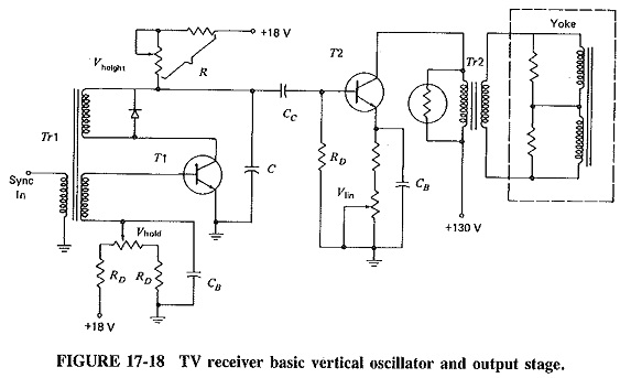
Vhold is the vertical hold control, with which positive bias on the base of T1 is adjusted. A glance at Figure 17-17 shows that this has the effect of adjusting VB – VI. In this fashion the voltage through which RC must discharge is varied, and so is the discharge period (indirectly). The vertical frequency, i.e., vertical hold, is varied.
As envisaged in the preceding section, the blocking oscillator transformer tertiary winding is used for the application of sync pulses. They are positive-going and used to initiate prematurely the conduction period of T1. This has the effect of controlling the period of the sawtooth, so that this is made equal to the time difference between adjoining vertical sync pulses. Note finally that a protective diode is used across the primary winding of Trl, in lieu of the load resistor across the tertiary in Figure 17-17.
Vertical Output Stage:
The vertical output stage is a power output stage with a transformer-coupled output, as shown by T2 and its associated circuitry in Figure 17-18. An additional amplifier is often used between the vertical oscillator and output stage. This driver generally takes the form of an emitter-follower, whose function is to isolate the oscillator and provide additional drive power for the output stage.
The Vertical Deflection Circuit in TV voltage from the vertical oscillator provides a linear rise in base voltage for the output stage, to produce a linear rise in collector current during trace time. The drive voltage cuts off the amplifier during retrace, causing the output current to drop to zero rapidly. The result is a sawtooth output current in the primary and secondary windings of the vertical output transformer Tr2, and this induces the saw-tooth deflection current in the vertical coils in the yoke. In actual practice, the situation is a little more complicated. The inductance of the coils and transformers must be taken into account, so that a certain amount of wave shaping must take place, with R-C components which have not been shown. Their function is to predistort the driving waveform, to produce the correct sawtooth deflection current in the yoke coils.
The V1in potentiometer is the vertical linearity control of the receiver, again located at the back of the receiver. Its adjustment varies the bias on the output transistor to obtain the optimum operating point. The thermistor across the primary winding of Tr2 stabilises the collector of T2, and the resistors across the yoke coils have the function of preventing ringing immediately after the rapid retrace. Their values are typically a few hundred ohms. if ringing is not prevented, the beam will trace up and down in the (approximately) top one-third of the screen, producing broad, bright horizontal bars in that area of the screen.
Note lastly the high supply voltage for the output transistor. This is needed to provide the large Vertical Deflection Circuit in TV swing required, of the order of 100 V peak to peak.