Define Suppression of Carrier:
Three main systems are employed for the generation of SSB; the filter method, the phase cancellation method and the “third method.” They differ from one another in the way of suppressing the unwanted sideband, but all use some form of balanced modulator to the Define Suppression of Carrier. The balanced modulator is the key circuit in single-sideband generation. The next section will illustrate the proof of its operation.
Effect of Nonlinear Resistance on Added Signals:
The relationship between voltage and current in a linear resistance is given by
![]()
where b is same constant of proportionality. If Equation (4-1) refers to a resistor, then b is obviously its conductance. If Equation (4-1) is made to apply to the collector current and base voltage of a transistor, i will be the collector current, and v will be the voltage applied to the base. If the amplifier operates in class A, there will also be a dc component of collector current (a), which is not dependent on the signal voltage at the base. We may write
![]()
where a is the dc component of the collector current, and b is the transconductance of the transistor.
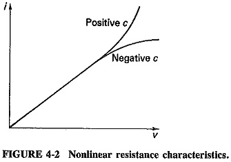
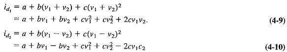
In a nonlinear resistance, the current is still to a certain extent proportional to the applied voltage, but no longer directly as before. If the curve of current versus voltage is plotted, as in Figure 4-2, it is found that there is now some curvature in it. The previous linear relation seems to apply up to a certain point, after which current increases more (or less) rapidly with voltage. Whether the increase is more or less rapid depends on whether the device begins to saturate, or else some sort of avalanche current multiplication takes place. Current now becomes proportional not only to voltage but also to the square, cube and higher powers of voltage. This nonlinear relation is most conveniently expressed as
![]()
The reason that the initial portion of the graph is linear is simply that the coefficient c is much smaller than b. A typical numerical equation might, well be something like i = 5 + 15ν + 0.2ν2, in which case curvature is insignificant until ν equals at least 3. Therefore, c in practical nonlinear resistances is much greater than d, which is in turn larger than the constants preceding the higher-power terms. Only the square term is large enough to be taken into consideration for most applications, so that we are left with
![]()
where a and b have the meanings previously given, and c is the coefficient of nonlinearity.
Since Equation (4-4) is generally adequate in relating the output current to the input voltage of a nonlinear resistance, it may now be applied to the gate-voltage-drain-current characteristic of a FET. If two voltages are applied simultaneously to the gate, then
Let the two input voltages be sinusoidal. We may then write
where ω and ρ are the two angular velocities. Substituting Equation (4-6) into (4-5), we have

Equation (4-7) may be simplified by the use of the appropriate trigonometrical expressions. (Note that these expressions are sin x sin y = 1/2 [cos (x — y) — cos (x + y)] and sin2 x = 1/2 (1 — cos 2x).
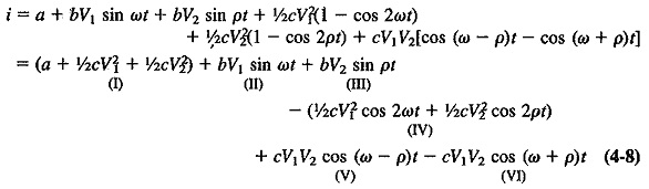
The previous derivation, with the resulting Equation (4-8), is possibly the most important of all in communications. It is the proof (1) that harmonic and intermodulation distortion may occur in audio and RF amplifiers, (2) that sum and difference frequencies will be present in the output of a mixer, (3) that the diode detector has audio frequencies in its output, (4) of the operation of the beat-frequency oscillator (BFO) and the product detector, and (5) that it is part of the proof that the balanced modulator produces AM with the Define Suppression of Carrier.
If in Equation (4-8) ω is taken as the carrier angular frequency, and p as the modulating angular frequency, then term I is the dc component, term II is the carrier, term III is the modulating signal, term IV consists of harmonics of the carrier and the modulation, term V represents the lower sideband voltage and term VI is the upper sideband. The equation shows that when two frequencies are passed together through a nonlinear resistance, the process of amplitude modulation takes place. In a practical modulation circuit, the voltages in Equation (4-8) would be developed across a circuit tuned to the carrier frequency, and with a bandwidth just large enough to pass the carrier and two sideband frequencies but no others.
The Balanced Modulator:
Two circuits of the balanced modulator are shown in Figure (4-3). Each utilizes the nonlinear principles just discussed. The modulation voltage ν2 is fed in push-pull, and the carrier voltage ν1 in parallel, to a pair of identical diodes or class A (transistor or FET) amplifiers. In the FET circuit, the carrier voltage is thus applied to the two gates in phase; whereas the modulating voltage appears 180° out of phase at the gates, since they are at the opposite ends of a center-tapped transformer. The modulated output currents of the two FETs are combined in the center-tapped primary of the push-pull output transformer. They therefore subtract, as indicated by the direction of the arrows in Figure 4-3b. If this system is made completely symmetrical, the carrier frequency will be completely canceled. No system can of course be perfectly symmetrical in practice, so that the carrier will be heavily suppressed rather than completely removed (a 45-dB Define Suppression of Carrier is normally regarded as acceptable). The output of the balanced modulator contains the two sidebands and some of the miscellaneous components which are taken care of by the tuning of the output transformers secondary winding. The final output consists only of sidebands.
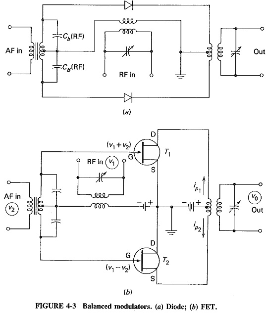
Since it is not immediately apparent how and why only the carrier is suppressed, a mathematical analysis of the balanced modulator is now given.
As indicated, the input voltage will be ν1 + ν2 at the gate of T1 (Figure 4-3b) and ν1 – ν2 at the gate of T2. If perfect symmetry is assumed (it should be understood that the two devices used in the balanced modulator, whether diodes or transistors, must be matched), the proportionality constants will be the same for both FETs and may be called a, b, and c as before. The two drain, currents, calculated as in the preceding section, will be
As previously indicated, the primary current is given by the difference between the individual drain currents. Thus
![]()
when Equation (4-10) is subtracted from (4-9).
We may now represent the carrier voltage ν1 by νc sin ωct and the modulating voltage ν2 by Vm sin ωmt. Substituting these into Equation (4-11) gives

The output voltage ν0 is proportional to this primary current. Let the constant of proportionality be α. Then
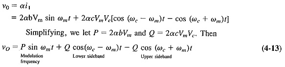
Equation (4-13) shows that (under ideally symmetrical conditions) the Define Suppression of Carrier has been canceled out, leaving only the two sidebands and the modulating frequencies.
The proof applies equally to both diagrams of Figure 4-3. The tuning of the output transformer will remove the modulating frequencies from the output, but it is also possible to suppress them by the action of the circuit. The addition of two more diodes to the diode balanced modulator is required for this result, and the circuit then becomes known as the ring modulator.