Electronic Devices and Circuits

Semiconductor Diode Specifications

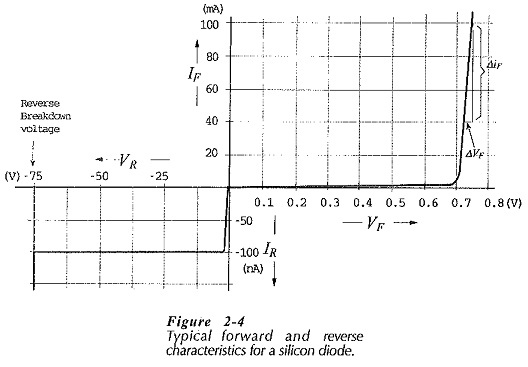
Semiconductor Diode Specifications: Diode Data Sheets – To select a suitable diode for a particular application, the data sheets, or Semiconductor Diode Specifications, provided by device manufacturers must be consulted. Portions of typical diode data sheets are shown in Fig. 2-21 . Most data sheets start off with the device type number at the top […]

Semiconductor Diode Specifications Read More »

Diode Approximations

Diode Approximations: Diode Approximations – As we know already that, a diode is essentially a one-way device, offering a low resistance when forward biased, and a high resistance when biased in reverse. An ideal diode (or perfect diode) would have zero forward resistance and zero forward voltage drop. It would also have an infinitely high

Diode Approximations Read More »

PN Junction Diode Working Principle

PN Junction Diode Working Principle: A PN Junction Diode Working Principle explains about the ability to permit substantial current flow when forward-biased, and to block current when reverse-biased. Thus, it can be used as a switch; on when forward-biased, and off when biased in reverse. In PN Junction Diode Working Principle, the copper wire connecting

PN Junction Diode Working Principle Read More »

PN Junction Forward Bias

PN Junction Forward Bias: Consider the effect of an external bias voltage applied with the polarity of PN Junction Forward Bias shown in Fig. 1-23; positive on the p-side, negative on the n-side. The holes on the p-side, being positively charged particles, are repelled from the positive terminal and driven toward the junction. Similarly, the

PN Junction Forward Bias Read More »

Reverse Bias PN Junction

Reverse Bias PN Junction: When an external bias voltage is applied to a pn-junction, positive to the n-side and negative to the pride, electrons from the n-side are attracted to the positive terminal, and holes from the p-side are attracted to the negative terminal. As shown in Fig. 1-21, holes on the p-side of the

Reverse Bias PN Junction Read More »

PN Junction Semiconductor

PN Junction Semiconductor: Two blocks of PN Junction Semiconductor material are represented in Fig. 1-17; one block is p-type material, and the other is n-type. The small circles in the p-type material represent holes, which are the majority charge carriers in p-type. The dots in the n-type material represent the majority charge carrier free electrons

PN Junction Semiconductor Read More »

Scroll to Top