Transistor Terminals (Emitter, Collector and Base)
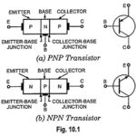
Transistor Terminals (Emitter, Collector and Base): As mentioned already, transistor is a single crystal in which there are two P-N junctions, as shown in Fig. 10.1. The idea behind is…
Zener Diode Terminals Articles: Construction and Working of Zener Diode: Zener diode, also sometimes called the breakdown diode, is a P-N junction diode specially designed for operation in the breakdown…
FET Transistor Articles: Junction Field Effect Transistor (JFET) – Construction, Symbols and Operation: Depending upon the majority charge carriers, Junction Field Effect Transistor (JFET) have been classified into two types,…
BJT Transistor Articles: Transistor Construction: The transistor construction consists of a silicon or germanium (preferably silicon because of its smaller cutoff current ICBO, smaller variations in ICBO due to variations…
Field Effect Transistors (FETs) Interview Questions and Answers: 1. What is the major difference between a bipolar and a unipolar device ? Ans. In a bipolar device, current conduction is by…
Transistor as a Switch Circuit Diagram and Working: The Transistor as a Switch Circuit Diagram and Working can be explained with the help of its output characteristics. Figure 31.2 shows…
Transistor Detector Circuit Working Principle: It is possible to achieve amplitude demodulation by using a three-element electronic device. A typical example of such a configuration is illustrated in Fig. 22.51.…
Darlington Pair Transistor - Circuit Diagram and its Workings: A very popular connection of two BJTs for operation as one "superbeta" transistor is the Darlington connection. In practice, the two…