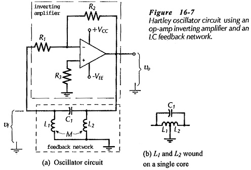
Hartley Oscillators using Op-Amp:
Hartley Oscillators using Op-Amp circuit is similar to the Colpitts oscillator, except that the feedback network consists of two inductors and a capacitor instead of two capacitors and an inductor. Figure 16-7(a) shows the Hartley Oscillators using Op-Amp circuit, and Fig. 16-7(b) illustrates the fact that L1 and L2 may be wound on a single core so that there is mutual inductance (M) between the two windings.
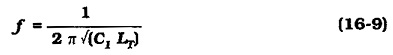
In this case, the total inductance is,
![]()
Oscillation occurs at the feedback network resonance frequency ;
The attenuation of the feedback network is
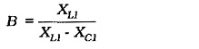
It can be shown that the required 180° phase shift occurs when
![]()
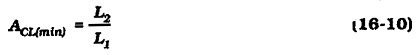
The loop gain must be a minimum of one, giving;
Design procedure for a Hartley Oscillators using Op-Amp circuit is similar to that for a Colpitts oscillator.
BJT Hartley Oscillator:
Figure 16-9 shows the circuit of a Hartley Oscillators using Op-Amp using a BJT amplifier. The basic circuit in Fig. 16-9(a) is similar to the op-amp Hartley oscillator, and its operation is explained in the same way as for the op-amp circuit. Note that coupling capacitors C2 and C4 are required to avoid dc grounding the transistor base and collector terminals through L1 and L2.
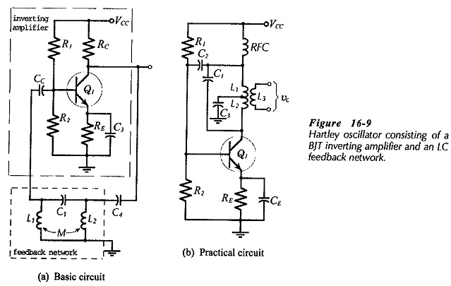
In the practical BJT Hartley Oscillators using Op-Amp circuit shown in Fig. 169(b) L1, L2, and C1 constitute the phase shift network. In this case, the inductors are directly connected in place of the transistor collector resistor (RC). The circuit output is derived from the additional inductor winding (L3). The radio frequency choke (RFC) passes the direct collector current, but ac isolates the upper terminal of L1 from the power supply. Capacitor C2 couples the output of the feedback network back to the amplifier input. Capacitor C4 at the BJT collector in Fig. 16-9(a) is not required in Fig. 16-9(b), because L2 is directly connected to the collector terminal. The Junction of L1 and L2 must now be capacitor coupled to ground (via C3) instead of being direct coupled.