555 Timer Circuit:
The timer IC 555 Timer Circuit is most versatile linear integrated device introduced by Signetics corporation in early 1970. It is basically a monolithic timer circuit which can be used in many applications such as monostable and astable multivibrators, linear ramp generator, missing pulse detector, pulse width modulator etc.
The IC 555 Timer Circuit combines the following elements :
- A relaxation oscillator
- RS flip flop
- Two comparators
- Discharge transistor
555 R-S Flip Flop Circuit Diagram:
The figure 2.96 shows the part of the basic RS flip flop circuit. It used a pair of cross coupled Transistors. Each Collector Drives the base of opposite transistor thorough a resistance RB. In such a Circuit, One transistor Operates in saturation while the other in cut off region. This if the transistor Q2 is in saturation then its collector voltage is zero. This voltage is the base drive of transistor Q1. So there is no base drive for Q1 and it goes into cut off. Thus its collector voltage is approximately +VCC. This drives the base of Q2 which ensures that the Q2 operates in saturation region.
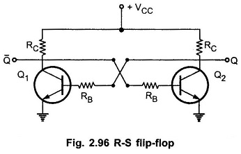
Now if transistor Q2 goes into cut off, its collector voltage approaches to +VCC which drives the transistor Q1 into saturation. This makes collector voltage of Q1 almost zero which keeps the transistor Q2 in cut off. So all the time, circuit ensures that one transistor operates in saturation and other in cut off.
The two outputs Q and Q̅ are taken from two collectors. Depending upon the transistor operation, the output value gets decided.
Now this basic circuit along with some additional components gives us a popular RS flip flop circuit. It has two inputs set (S) and reset (R). With the help of these inputs, the output Q can be made high or low. Depending on Q, complementary will be the value of output Q̅ i.e. low or high.
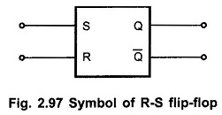
The Fig. 2.97 shows the symbol of RS flip flop circuit. When input set (S) is high, the output Q is high and Q̅ is low. The high reset (R) input resets the output Q to low. The output Q remains in its state of high or low unless and until it is triggered externally into the opposite state.
The Table 2.5 shows the state of output Q related to inputs S and R.
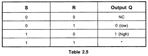
S = Set, R = Reset, NC = No Change, * = Race
To understand the operation of IC 555 Timer Circuit, let us study the basic timing concept using RS flip flop circuit.
Basic Timer Circuit:
The Fig. 2.98 shows the Basic Timer Circuit, which uses R S Flip Flop Circuit along with some other elements.
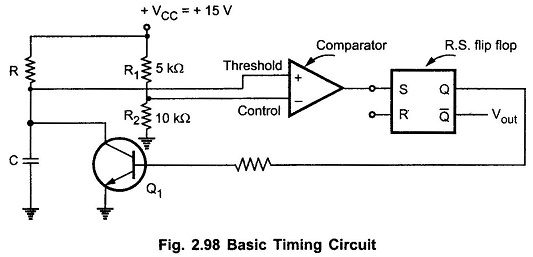
To understand the operation, consider that the output Q is high. This drives the base of Q1 and as it is high it drives Q1 into saturation. It makes the capacitor voltage zero and as other end of capacitor is grounded, the capacitor is shorted. In this condition it can not be charged.
The circuit uses a comparator. The noninverting input of comparator is called threshold voltage. While its inverting input is called control voltage. The R1 and R2 forms a potential divider which maintains control voltage constant at +10V. As Q is high and transistor Q1 is in saturation, the threshold voltage is zero.
As R1 = 5 kΩ and R2 = 10 kΩ
![]()
Now if high voltage is applied to the reset (R) input of flip-flop then it resets R-S flip-flop and output Q goes low. This drives the transistor Q1 in cut off. Now the capacitor is free to charge and starts charging through resistance R. The threshold voltage thus starts increasing. When it becomes just greater than +10V which is the control voltage, the comparator output goes high. This high signal is driving the set (S) input of R-S flip flop. This changes the state of output Q back to high. This drives transistor Q1 into saturation which quickly discharges the capacitor C.
Waveforms of Basic Timing Circuit:
The Fig. 2.99 shows the waveforms of threshold voltage and output voltage Vout. The charging of capacitor is exponential hence the threshold voltage is also exponential in nature. When Q goes low, the Q̅ becomes high and positive going pulse appears at Vout. Similarly when capacitor voltages increases more than the control voltage, Q becomes high and Q̅ becomes low. This brings Vout to zero instantly. Thus a rectangular output gets produced.
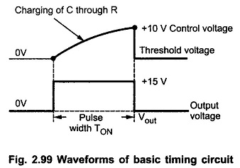
It can be observed that output remains high for the time which is required by the capacitor to charge upto control Voltage, through R. Thus by varying R or C, the output pulse width can be varied. This is the working principle of timer IC 555 Timer Circuit.
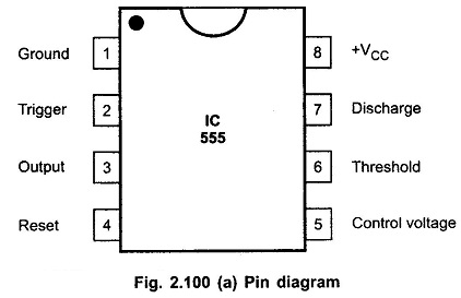
IC 555 Pin Diagram:
The Fig. 2.100 (a) and (b) show the IC 555 Pin Diagram and the IC 555 Timer Block Diagram. This is 8 pin IC timer.
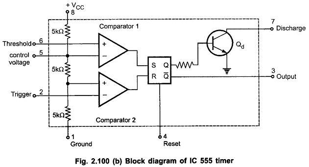
Block Diagram of 555 Timer:
Functions of Pins of IC 555 Timer:
The pin numbers of Timer IC 555 and their functions are discussed below :
Pin 1 : Ground
All the voltages are measured with respect to this terminal.
Pin 2 : Trigger
The IC 555 uses two comparators. The voltage divider consists of three equal resistances. Due to voltage divider, the voltage of noninverting terminal of comparator 2 is fixed at VCC/3. The inverting input of comparator 2 which is compared with VCC/3, is nothing but trigger input brought out as pin number 2. When the trigger input is slightly less than VCC/3 the comparator 2 output goes high. This output is given to reset input of R-S flip-flop. So high output of comparator 2 resets the flip-flop.
Pin 3 : Output
The complementary signal output (Q̅) of the flip-flop goes to pin 3 which is the output. The load can be connected in two ways. One between pin 3 and ground while other between pin 3 and pin 8.
Pin 4 : Reset
This is an interrupt to the timing device. When pin 4 is grounded, it stops the working of device and makes it off. Thus, pin 4 provides on/off feature to the IC 555. This reset input overrides all other functions within the timer when it is momentarily grounded.
Pin 5 : Control Voltage Input
In most of the applications, external control voltage input is not used. This pin is nothing but the inverting input terminal of comparator 1. The voltage divider holds the voltage of this input at 2/3 VCC. This is reference level for comparator 1 with which threshold is compared. If reference level required is other than 2/3 VCC for comparator 1 then external input is to be given to pin 5.
If external input applied to pin 5 is alternating then the reference level for comparator 1 keeps on changing above and below 2/3 VCC. Due to this, the variable pulse width output is possible:, This is called pulse width modulation, which is possible due to pin 5.
Pin 6 : Threshold
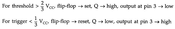
This is the noninverting input terminal of comparator 1. The external voltage is applied to this pin 6. When this voltage is more than 2/3 VCC, the comparator 1 output goes high. This is given to the set input of R-S flip-flop. Thus high output of comparator 1 sets the flip-flop. This makes Q of flip-flop high and Q low. Thus the output of IC 555 at pin 3 goes low.
Remember that output at pin 3 is Q̅ which is complementary output of flip-flop. In short,
Pin 7 : Discharge
This pin is connected to the collector of the discharge transistor Qd. When the output is high then Q is low and transistor Qd is off. It acts as an open circuit to the external capacitor C to be connected across it, so capacitor C can charge as described earlier. When output is low, Q is high which drives the base of Qd high, driving transistor Qd in saturation. It acts as short circuit, shorting the external capacitor C to be connected across it.
Pin 8 : Supply +VCC
The IC 555 Timer Circuit can work with any supply voltage between 4.5 V and 16 V.
Important Features of IC 555 Timer:
The various Important Features of IC 555 Timer Circuit are :
- The 555 is a monolithic timer device which can be used to produce accurate and highly stable time delays or oscillation. It can be used to produce time delays ranging from few microseconds to several hours.
- It has two basic operating modes : monostable and astable
- It is available in three packages : 8-pin metalcan, 8-pin mini DIP or a 14-pin DIP. A 14-pin package is IC 556 which consists of two 555 timers.
- The NE 555 (Signetics) can operate with a supply voltage in the range of 4.5 V to 18 V and is capable of sourcing and sinking output currents of 200 mA. Its CMOS version (TLC 555) can operate over a supply range of 2V to 18V and has output current sinking and sourcing capabilities of 100 mA and 10 mA, respectively.
- It has a very high temperature stability, as it is designed to operate in the temperature range of -55° to 125° C.
- Its output is capatible with TTL, CMOS and Op-Amp circuits.
Connecting Load to IC 555:
The output of 555 is used to drive load (controlling devices) such as transistors and relays. There are two ways of connecting load to output terminal : either between output terminal (pin 3) and ground (pin 1) or between output terminal (pin 3) and supply voltage (pin 8) as shown in Fig. 2.101.
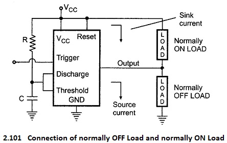
Normally output is low. Thus, load current flows through the load connected between VCC and output terminal. The load connected in this way is called normally ON LOAD and load current is called the sink current. However, the current through the grounded load is zero when the output is low. Thus, the load connected between output terminal and ground is called normally OFF LOAD. On the other hand, when the output is high, the current through the load connected between VCC and output terminal is zero. However, the output terminal supplies current to the normally off load. This current is called the source current. In 555 timer maximum value of sink or source current is 200 mA.