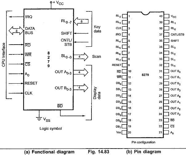
Interfacing ICs

Pin Diagram of 8279

Pin Diagram of 8279: Fig. 14.83 shows functional and pin diagram of 8279. It is a 40 pin device and looking at Fig. 14.83 (a) we can see that these pins are divided in four functional groups : CPU interface Key data Display data Scan CPU Interface Pins: As shown in Fig. 14.83 (a), it […]

Pin Diagram of 8279 Read More »

Features of Intel 8279 Programmable Keyboard Display Interface

Features of Intel 8279 Programmable Keyboard Display Interface: The Intel 8279 is a general purpose programmable keyboard and display I/O interface device designed for use with Intel microprocessors. The Features of Intel 8279 Programmable Keyboard Display Interface are 1. It provides a scanned interface to a 64-contact key matrix, with two more keys CONTROL and

Features of Intel 8279 Programmable Keyboard Display Interface Read More »

8259 Programmable Interrupt Controller

8259 Programmable Interrupt Controller: The 8259 Programmable Interrupt Controller requires two types of command words. Initialization Command Words (ICWs) and Operational Command Words (OCWs). The 8259 Programmable Interrupt Controller can be initialized with four ICWs; the first two are compulsory, and the other two are optional based on the modes being used. These words must

8259 Programmable Interrupt Controller Read More »

Interfacing 8259 with 8085

Interfacing 8259 with 8085: Fig. 14.72 shows Interfacing 8259 with 8085 microprocessor system. Addressing of 8259A : The 74LS138 address decoder will assert the CS input of the 8259A when an I/O base address is F0H or F1H on the address bus. The A0 input of the 8259A is used to select one of the

Interfacing 8259 with 8085 Read More »

8259 Block Diagram

8259 Block Diagram: Fig. 14.71 shows the internal 8259 Block Diagram. It includes eight blocks : data bus buffer, read/write logic, control logic, three registers (IRR, ISR and IMR), priority resolver, and cascade buffer. Data Bus Buffer: The data bus buffer allows the 8085 to send control words to the 8259A and read a status

8259 Block Diagram Read More »

Interfacing of 8257 with 8085

Interfacing of 8257 with 8085: Fig. 14.68 shows the interfacing of 8257 with 8085 in I/O mapped I/O technique. In slave mode, RD and WR signals are activated by CPU when IO/M signal is high, indicating I/O bus cycle. In master mode DMA controller: (8257) generates MEMR,MEMW, IOR and IOW signals to control the data

Interfacing of 8257 with 8085 Read More »

Operating Modes of 8257

Operating Modes of 8257: The Operating Modes of 8257 can be programmed to operate in following modes : Rotating Priority Mode : In rotating priority mode, the priority of the channels has a circular sequence. In this, channel being serviced gets the lowest priority and the channel next to it gets the highest priority as

Operating Modes of 8257 Read More »

8257 Pin Diagram

8257 Pin Diagram: Fig. 14.61 shows 8257 Pin Diagram. Data Bus (D0-D7) : These are bi-directional tri-state signals connected to the system data bus. When CPU is having control of system bus it can access contents of address register, status register, mode set register, and a terminal count register and it can also program, control

8257 Pin Diagram Read More »

Scroll to Top