Bipolar Junction Transistors

Transistor Testing Circuit

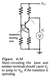
Transistor Testing Circuit: In-Circuit Testing – A quick test to check if a transistor is operational can be performed while the device is still connected in a circuit. Consider Fig. 4-34, which shows a voltmeter connected to measure the transistor collector voltage (VC). The VC measurement is noted, then the base and emitter terminals are temporarily […]

Transistor Testing Circuit Read More »

Common Collector Characteristics of BJT

Common Collector Characteristics of BJT: In the Common Collector Characteristics of BJT circuit arrangement of Fig. 4-31, the collector terminal is common to both input CB voltage and output CE voltage. Using this circuit, the common-collector input, output, and current gain characteristics can be determined. The output and current gain characteristics are shown in Fig.

Common Collector Characteristics of BJT Read More »

CE Transistor Characteristics

CE Transistor Characteristics: Common Emitter Circuit – Figure 4-26 shows a circuit for determining CE Transistor Characteristics. The input voltage is applied between the B and E terminals, and the output is taken at the C and E terminals. The emitter terminal is common to both input and output. Voltage and current levels are measured

CE Transistor Characteristics Read More »

Common Base Transistor Characteristics

Common Base Transistor Characteristics: To investigate the Common Base Transistor Characteristics of a diode (a two-terminal device), several levels of forward or reverse bias voltage are applied and the resulting current levels are measured. The characteristics of the device are then derived by plotting the graph of current versus voltage. Because a transistor is a

Common Base Transistor Characteristics Read More »

Amplification in Transistor

Amplification in Transistor: Current Amplification in Transistor – We already know that a transistor can be used for current amplification. A small change in the base current (ΔIB) produces a large change in collector current (ΔIC) and a large emitter current change (ΔIE), [see Fig. 4-16(a) and (b)]. Rewriting Eq. 4-5, the current gain from the

Amplification in Transistor Read More »

Transistor Voltage and Current

Transistor Voltage and Current: The Transistor Voltage polarities for an npn transistor are shown in Fig. 4-10(a). As well as conventional current direction, the direction of the arrowhead indicates the transistor bias polarities. For an npn transistor, the base is biased positive with respect to the emitter, and the arrowhead points from the (positive) base

Transistor Voltage and Current Read More »

Transistor Operation

Transistor Operation: pnp and npn Transistor Operation – A junction transistor is simply a sandwich of one type of semiconductor material (p-type or n-type) between two layers of the opposite type. A block representation of a layer of p-type material between two layers of n-type is shown in Fig. 4-1(a). This is described as an npn

Transistor Operation Read More »

Scroll to Top