Coupling and Bypassing Capacitors:
Coupling Capacitors – To use a transistor circuit to amplify or otherwise process an ac signal, the signal source must be connected to the circuit input. If the source is directly connected to the input, as illustrated in Fig. 6-1(a), the circuit bias conditions will be altered. Figure 6-1(b) shows that the signal source resistance (rs) is in parallel with voltage divider resistor R2 when the signal is directly connected to the circuit in the Coupling and Bypassing Capacitors Coupling.
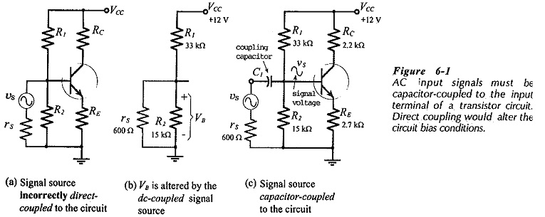
Thus, the bias voltage is altered to,
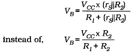
Figure 6-1(c) shows the use of capacitor C1 to couple the/ signal source to the circuit input. Because C1 is an open-circuit to direct currents, rs does not affect the level of VB. Capacitor C1 behaves as a short-circuit for the ac signals, so that the signal voltage (vS) appears at the transistor base, as illustrated. In this case, the signal is said to be ac coupled to the circuit input, and C1 is referred to as a coupling-capacitor. Input coupling capacitors are normally used with all types of bias circuits, otherwise the circuit bias conditions will be altered.
A coupling capacitor is usually required at the output of a transistor circuit (as well as at the input) to couple to a load resistor, or to another amplification stage. Figures 6-2(a) and (b) show the effect of directly coupling a load (RL) to the circuit output. The supply voltage at the transistor collector terminal is reduced from VCC to,
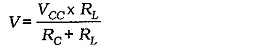
and the collector resistance becomes,
![]()
This has the effect of altering the circuit dc load line and Q-point.
The use of an output coupling capacitor (C2) is illustrated in Fig. 6-2(c). Like the input coupling capacitor, C2 offers a dc open circuit and behaves as an ac short-circuit. Thus, it passes the output waveform to the load without affecting the circuit bias conditions.
AC Degeneration:
In the discussion on collector-to-base bias, it was explained that an increase in IB would produce a decrease in VCE, and this would tend to cancel the original increase in IB. This, of course, is an effect that produces good bias stability, however, this same reaction occurs when an ac signal is applied to the circuit input for amplification. The voltage change at the transistor collector (produced by the ac input) is fed back to the base where it tends to partially cancel the signal. The effect is termed ac degeneration, and it can result in a very low voltage gain.
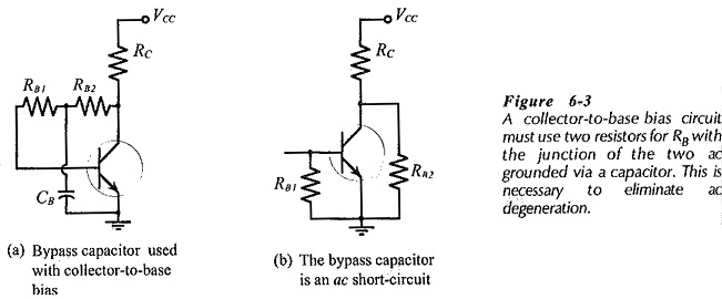
Figure 6-3(a) shows how ac degeneration is eliminated in collector-to-base bias circuits. RB is replaced with two approximately equal resistors (RB1 and RB2), which add up to RB. A bypass capacitor (CB) is connected from the junction of RB1 and RB2 to the ground terminal, as illustrated. Capacitor CB offers a short-circuit to ac signals, so that there is no feedback from the transistor collector to the base. Figure 6-3(b) shows that, when CB is replaced with a short-circuit, RB1 and RB2 appear in parallel with the circuit input and output respectively. Because they are large-value resistors, they do not affect the circuit voltage gain
Emitter Bypassing:
Voltage divider bias circuits also suffer ac degeneration because of the presence of the emitter resistor (RE). In this case, the ac signal voltage is developed across RE and the transistor BE junction in series, instead of just across the BE junction alone. The problem is eliminated by the emitter bypass capacitor (CE) illustrated in Fig. 6-4, which provides an ac short-circuit across RE.
Capacitor polarity:
Bypass capacitors are usually polarized (electrolytic-type), and Coupling and Bypassing Capacitors Coupling can also be polarized, so it is very important that capacitors are correctly connected. As discussed already, incorrectly connected polarized capacitors can explode! Also, electrolytic capacitors tend to have a high leakage current when incorrectly connected, so even if they do not explode, they can affect circuit bias conditions The positive terminal must be connected to the more positive of the two circuit points where the capacitor is installed.
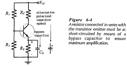
The capacitor positive terminal is represented by the straight line on the capacitor symbol, or is identified by the plus sign on the alternative capacitor symbol, (see Fig 6-4). The transistor emitter terminal in Fig. 6-4 is more positive than ground level, as illustrated. Consequently, the positive terminal of the emitter bypass capacitor is connected at the transistor emitter, and the negative terminal goes to ground.
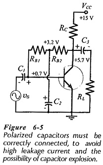
Figure 6-5 shows a circuit with correctly-connected Coupling and Bypassing Capacitors Coupling. The dc voltage level at the right side of C1 is +0.7 V, and the left side is grounded via the signal source. So, the polarity is plus on the right, minus on the left. The voltage at the junction of resistors RB1 and RB2 is +3.2 V, consequently, the positive terminal of C2 must be connected at that point, and C2 negative terminal is grounded. Output coupling capacitor C3 has its left side at +5.7 V, and the right side is grounded via RL, requiring the capacitor to be connected as illustrated.