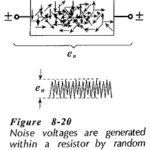
Transistor Circuit Noise
Transistor Circuit Noise: Unwanted signals at the output of an electronics system are termed noise. The noise amplitude may be large enough to severely distort, or completely swamp, the wanted…
Continue Reading
Transistor Circuit Noise