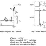
Biasing FET Switching Circuits
Biasing FET Switching Circuits: JFET Switching - A Biasing FET Switching Circuits is normally in an off state with zero drain current, or in an on state with a very…
Continue Reading
Biasing FET Switching Circuits
Biasing FET Switching Circuits: JFET Switching - A Biasing FET Switching Circuits is normally in an off state with zero drain current, or in an on state with a very…
FET Transistor Articles: Junction Field Effect Transistor (JFET) – Construction, Symbols and Operation: Depending upon the majority charge carriers, Junction Field Effect Transistor (JFET) have been classified into two types,…
FET Biasing Articles: DC Load Line for FET: The DC Load Line for FET circuit is drawn on the device output characteristics (or drain characteristics) in exactly the same way…
Electronic Devices and Circuits Articles: This Electronic Devices and Circuits Articles which includes the following topics: Introduction to Semiconductor Materials and Devices Conduction in Solids Conductor Semiconductor and Insulator P…
Electronics Communication Engineering viva Questions and Answers: Following are the Basic and Advanced Electronics Communication Engineering viva Questions and Answers Acceptor atoms - Trivalent atoms that accept free electrons from…
Electronics Engineering Multiple Choice Questions and Answers (MCQs) Part 4: 150. In phase modulation, phase deviation is proportional to (a) carrier amplitude. (b) carrier phase. (c) message signal. (d) message…
Electronics Engineering Interview Questions and Answers: 555 IC Timer Interview Questions and Answers Active Filters Interview Questions and Answers Amplifier Frequency Response Interview Questions and Answers Basic DC Circuit Analysis…
Power Semiconductor Devices Interview Questions and Answers: 1. Give the broad classification of power semiconductor devices. Ans. Power semiconductor devices can be broadly classified into three categories viz. power diodes, thyristors…