Read Only Memory (ROM):
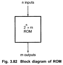
A Read Only Memory (ROM) is a device that includes both the decoder and the OR gates within a single IC package. The Fig. 3.82 shows the block diagram of ROM. It consists of n input lines and m output lines. Each bit combination of the input variables is called an address. Each bit combination that comes out of the output lines is called a word. The number of bits per word is equal to the number of output lines, m. The address specified in binary number denotes one of the minterms of n variables. The number of distinct addresses possible with n input variables is 2n. An output word can be selected by a unique address, and since there are 2n distinct addresses in a ROM, there are 2n distinct words in the ROM. The word available on the output lines at any given time depends on the address value applied to the input lines.
Let us consider 64 x 4 ROM. The Read Only Memory consists of 64 words of 4 bits each. This means that there are four output lines and particular word from 64 words presently available on the output lines is determined from the six input lines. There are only six inputs in a 64 x 4 ROM because 26 = 64, and with six variables, we can specify 64 addresses or minterms. For each address input, there is a unique selected word. Thus, if the input address is 000000, word number 0 is selected and applied to the output lines. If the input address is 111111, word number 63 is selected and applied to the output lines.
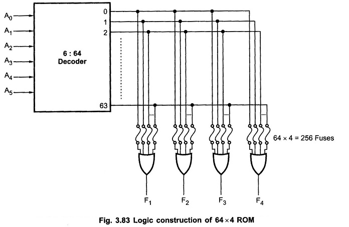
The Fig. 3.83 shows the internal logic construction of a 64 x 4 ROM. The six input variables are decoded in 64 lines by means of 64 AND gates and 6 inverters. Each output of the decoder represents one of the minterms of a function of six variables. The 64 outputs of the decoder are connected through fuses to each OR gate. Only four of these fuses are shown in the diagram, but actually each OR gate has 64 inputs and each input goes through a fuse that can be blown as desired.
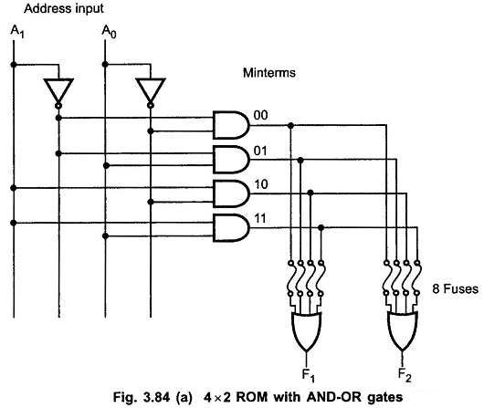
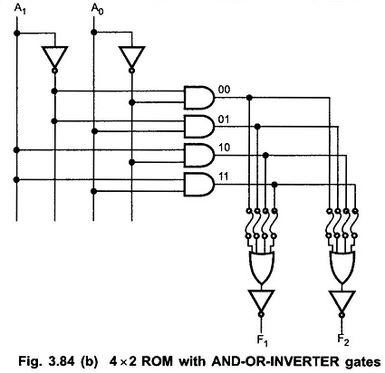
The ROM is a two level implementation in sum of minterms form. Let us see AND-OR and AND-OR-INVERTER implementation of ROM. Fig. 3.84 shows the 4 x 2 ROM with AND-OR and AND-OR-INVERTER implementations.
Combination Logic Implementation Using ROM:
Looking at the logic diagram of the ROM, we can realize that each output provides the sum of all the minterms of n input variables. We know that any Boolean function can be expressed in sum of minterms form. By breaking the links of those minterms not included in the function, each ROM output can be made to represent the Boolean function of one of the output variables in the combinational circuit. For an n-input, m-output combinational circuit, we need a 2n x m ROM. See in Fig. 3.84(a) & (b).