Reactive Plasma Etching:
The reactive plasma is the discharge in which gases ionized producing chemically active species, oxidizers, reagents. The plasma is reactive in both gaseous and solid phase, hence the name is Reactive Plasma. These plasmas are used to remove the materials from the surfaces which are not masked by the lithographic patterns. The process is called Etching. Hence the etching of unwanted material with the interactions of plasmas forming volatile product is called Reactive Plasma Etching.
Reactive Plasma Etching also serves to form the, interconnections between the various mask levels and patterns the opaque sections of the masks. The main objective of the etching is removal by proper etchant, minimum removal of masking resist and high throughput.
Wet Etching:
In early days wet etching was the most widely used process. The main advantage of wet etching is high throughput. The wet etchants like nitric acid and hydrofluoric acids attack and remove the layer to be etched. The high throughput can be achieved by immersing large number of wafers in the etchant simultaneously. The main disadvantage of the wet etching is its isotropic nature.
Wet etching penetrates horizontally as well as vertically. The lateral etch cuts the resist and widens the layer to be formed on the substrate. The virtual parameter of the etching is selectivity. For higher selectivity, the etching is better. Also it minimizes lateral removal of resist and over etching of substrate material. In wet etching, the etching rate is highly temperature dependent.
Reactive Ion Etching:
Now a days dry etching including Reactive Ion Etching (RIE) mode is widely used. The plasma reactor is as shown in the Fig. 1.9.
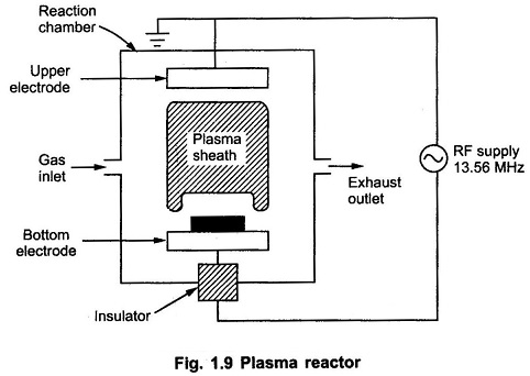
A radio frequency source operating at B.56 MHz produces a plasma discharge in a reaction chamber. The pressure in the reaction chamber is maintained in the range 3 to 150 mT. The plasma is a collection of electrons, positive ions, negative ions and the molecules produced by the interaction of introduced gases (containing halogen atoms) and the A.C. field externally applied. Note that the number of negative ions in the plasma is less, so that the electrons and positive ions are almost equal in number. Near the electrodes, the electron population is weakened producing a dark space called sheath near each electrode. Between the plasma and electrodes, a high voltage is developed which plays vital role in RIE mode. Due to the reaction of silicon and dielectric layers with fluorine or chlorine, halogenated layers are formed. Reactive Plasma Etching takes place with arrangement in which the radio frequency supply is connected to electrode and wafers placed on grounded electrode. By controlling the gas flow through the inlet, etch rate can be controlled. Generally wafers are arranged vertically. For precise and small dimensions of the structures, anisotropic etching is achieved with RIE.
For submicron VLSI, reactive ion beam etching (RIBE) is encorporated. In this technique, the reaction chamber and beam generating sections are isolated as the accelerating section drives reactive ions into the wafer surface.
Feature Size Control and Anisotropic Etching Mechanisms:
1. Pattern Transfer:
During the process of IC fabrication, patterned layers of different materials are formed on the silicon wafer surface. In general these layers interlace between insulators and conductors. In the insulating layer pattern, the layer covers almost complete surface with some windows in the layer. In such windows devices are formed or the contacts can be made. In the conducting layer pattern, the layer appears as series of lines. The lines are useful in connecting the terminals of active devices through the windows in the insulator and serving as interconnects between the devices.
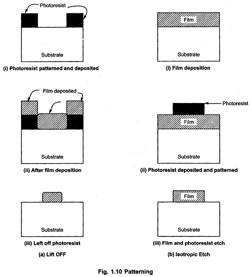
The pattern transfer process is associated with two techniques. In the first technique, first of all patterned resist film is formed. Then the layer is deposited over it. It is also called blanket deposition. Then by dissolving the resist, the unwanted material lifts off as shown in Fig. 1.10 (a). Hence this technique is known as lift off technique.
There are two drawbacks of this technique:
- The deposited profile made by this technique has rounded top.
- The deposition technique is limited below 200-300∘C.
To overcome these drawbacks generally etching technique is used for pattern transfer. Here first substrate is deposited forming a deposit layer. Then the pattern resist is formed over the substrate. The layer is then etched using resist as a mask. The etching process is said to be isotropic if the etching process attacks the layer surface equally in all directions. The schematic representation of etching technique is as shown in the Fig. 1.10 (b)
In general all the liquids are isotropic with the use of isotropic etching undercutting of the mask and narrowing of the feature takes place. The designed feature size can be achieved by making mask larger, if the amount with which feature narrows in isotropic etch is known. Such patterns are as shown in the Fig. 1.11.
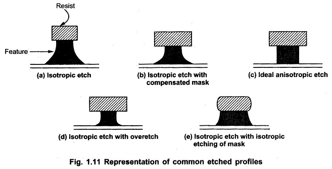
If the etching of a layer is faster in vertical direction than that in horizontal direction etching is called Anisotropic Etching.
2. Ion Enhanced and Ion Induced Etching:
In the beginning of this section, we have already studied that ion enhanced etching or ion induced etching takes place when ions are accelerated across plasma sheath under radio frequency conditions. Also the ions are accelerated only in vertical direction. The surfaces to be applied for etching are arranged horizontally. But still some ions travel horizontally because of horizontal component of velocity. Such component is combination of the thermal velocities and collisions of ions within plasma sheath. The ion beam is considered to travel vertically, so that wafer experiences ion bombardment. Such processes are effective in anisotropic etching.
3. Recombinant Species Mechanism:
Phosphorus doped silicon can be etched isotropically in Cl2 plasma. But if C2F6 is used as source gas, the same silicon can be etched anisotropically.
First consider the dissociation of the two gases in the plasma caused due to electron.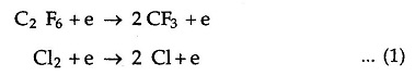
Then there are two main interactions take place at the surface namely etching and recombination represented by,
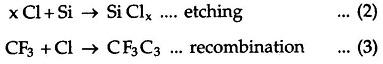
This reaction represented by equation (3) is dominant on the sidewalls of the feature. This shows that in the presence of the etch, the recombinent acts as sidewall passivant.
4. Sidewall Mechanism:
During the Reactive Plasma Etching process sometimes films are formed on the side walls of feature. These are of passivating type. Means these layers protect features from etching agents. Such sidewall depositions can be obtained from two mechanisms. In the first mechanism, the polymeric material is deposited which forms unsaturated CF2 radicals. In the second mechanism the etch product species stick and react with surface which are not exposed to ion bombardment.
5. Edge Profile Influencing Effects:
The sputtering rates are dependent on the angle of incidence of ions. In general, for most of the materials the angle is between 0 to 90°. Because of this surface sputtering takes place inclined to the angle of incidence. The physical sputtering of original resist feature is called faceting. And the inclined surface is called facet. When the edge of facet is directed downwards to the etching layer, then the taper is observed on the feature as shown in the Fig. 1.12.
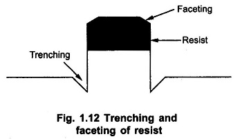
Trenching is a phenomenon related to ion energy in which the etch rate enhances in the vicinity of masked feature. Trenching takes place by two mechanisms. In the first mechanism, the ions reflected from resist with low angles, forms very high flux at the walls of feature. This is possible with the ions moving horizontally which cause slight taper in sidewall.
In second mechanism, the bending electric field enhances ion flux at the feature edges, leading to trenching. But this mechanism is observed in conductors only.