Biasing FET Switching Circuits
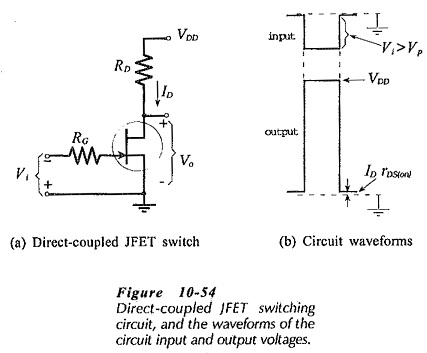
Biasing FET Switching Circuits: JFET Switching - A Biasing FET Switching Circuits is normally in an off state with zero drain current, or in an on state with a very small drain-source voltage. When the…
Comments Off on Biasing FET Switching Circuits
February 20, 2019